HBM is the wide road next to the GPU
A faster GPU needs more data. GDDR can run very fast, but it is like a highway with too few lanes and long routes on the board.
HBM changes the shape of the road: it puts memory close to the GPU and gives it a much wider interface through advanced packaging and TSV-based stacks.
First remember the simple tradeoff: shorter distance, wider bus, harder packaging. The details of interposers, TSVs, HBM3E, and HBM4 fit into that line.
A GPU is only fast when data arrives on time
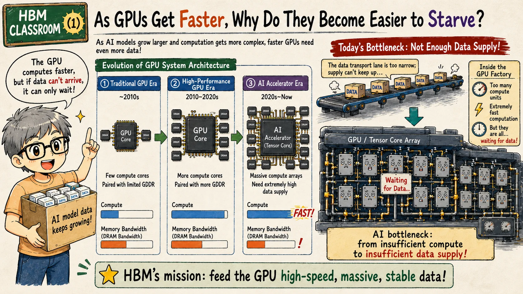
The first page starts from the most important system idea: a GPU or AI accelerator can contain enormous arithmetic capability, but those compute units are useful only when operands arrive on time. If model weights, activations, attention data, or intermediate tensors cannot reach the tensor-core array quickly enough, the accelerator stalls while silicon resources sit idle.
This is the memory-wall problem in a visual form. As GPU compute throughput grows, the data-supply system must grow with it. Otherwise the bottleneck moves from insufficient compute to insufficient data movement. In AI training and large-model inference, this affects utilization, tokens per second, training throughput, energy efficiency, and total cost of ownership.
HBM's mission is to feed the GPU with high-speed, massive, stable data. It does this not mainly by making DRAM clocks extreme, but by moving stacked DRAM close to the compute die and connecting it through a very wide, short interface. The package becomes part of the memory system.
The engineering lesson is that memory bandwidth is not a secondary feature. For modern accelerators, it is part of the compute architecture. More tensor cores only help when the memory subsystem can keep them supplied.
GDDR is fast, but the road becomes too narrow
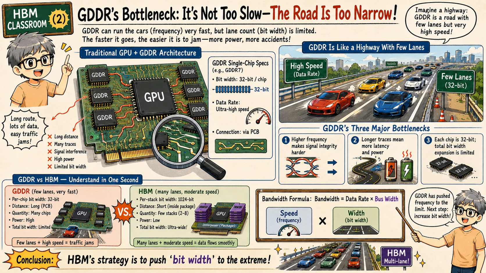
The second page explains why conventional GDDR is not simply 'bad memory.' GDDR can run at very high data rates, and it has been extremely successful for graphics and many accelerator systems. The limitation is physical scaling: each memory device has limited bus width, and the connection usually travels through package pins and PCB traces.
To increase total bandwidth with GDDR, designers add more devices, raise signaling speed, widen routing, and make the board work harder. That creates pressure on signal integrity, routing congestion, power delivery, board area, electromagnetic noise, and thermal design. The system becomes a fast road with too few lanes.
The useful formula is bandwidth equals data rate times bus width. GDDR leans heavily on data rate. HBM leans heavily on bus width. Instead of driving fewer lanes at extreme speed, HBM creates many short parallel lanes inside the package.
This explains why HBM can deliver excellent bandwidth per watt. Shorter links, lower I/O swing, and massive parallelism let the memory system move more data with less energy per bit, which is exactly what AI and HPC accelerators need.
HBM packages the GPU and memory together
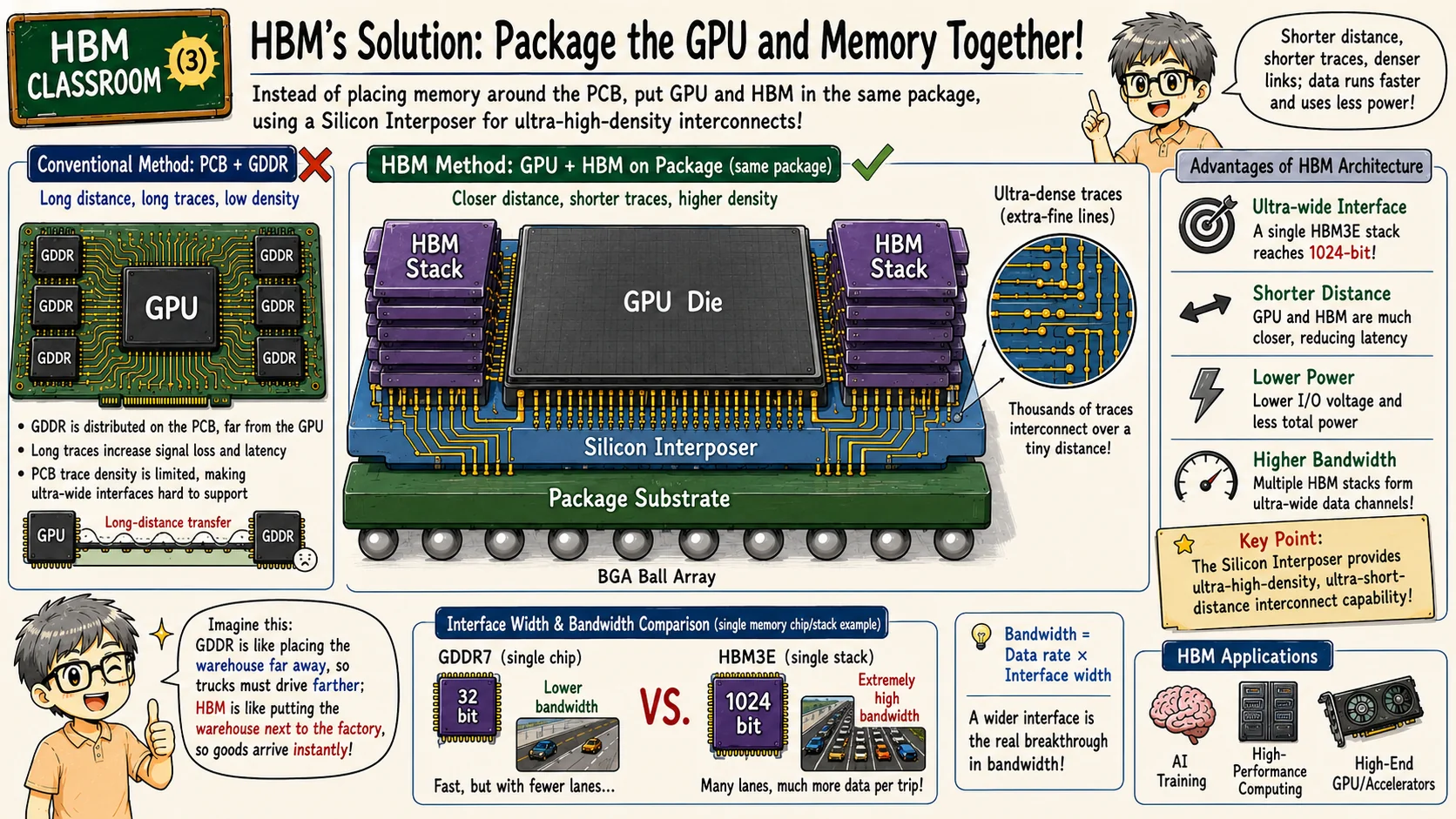
The third page moves from board-level memory to package-level integration. HBM places stacked DRAM beside the GPU die in the same advanced package. A silicon interposer or equivalent high-density interconnect layer provides thousands of fine connections between the logic die and the HBM stacks.
The interposer is the hidden highway. It gives the package wiring density that a normal PCB cannot provide at the same scale. Because the memory sits close to the GPU, the traces are shorter, the interface can be much wider, and the I/O energy can be lower.
This is why HBM is inseparable from advanced packaging terms such as CoWoS, 2.5D integration, silicon interposer, micro-bump, package substrate, and thermal solution. HBM is not just a DRAM part; it is a memory-plus-package architecture.
The tradeoff is complexity. Once memory moves into the package, yield, warpage, bonding quality, known-good-die handling, test coverage, thermal path, substrate routing, and packaging capacity all become part of the memory architecture. HBM bandwidth is created by the full integration stack, not by DRAM alone.
TSVs turn stacked DRAM into a vertical memory block
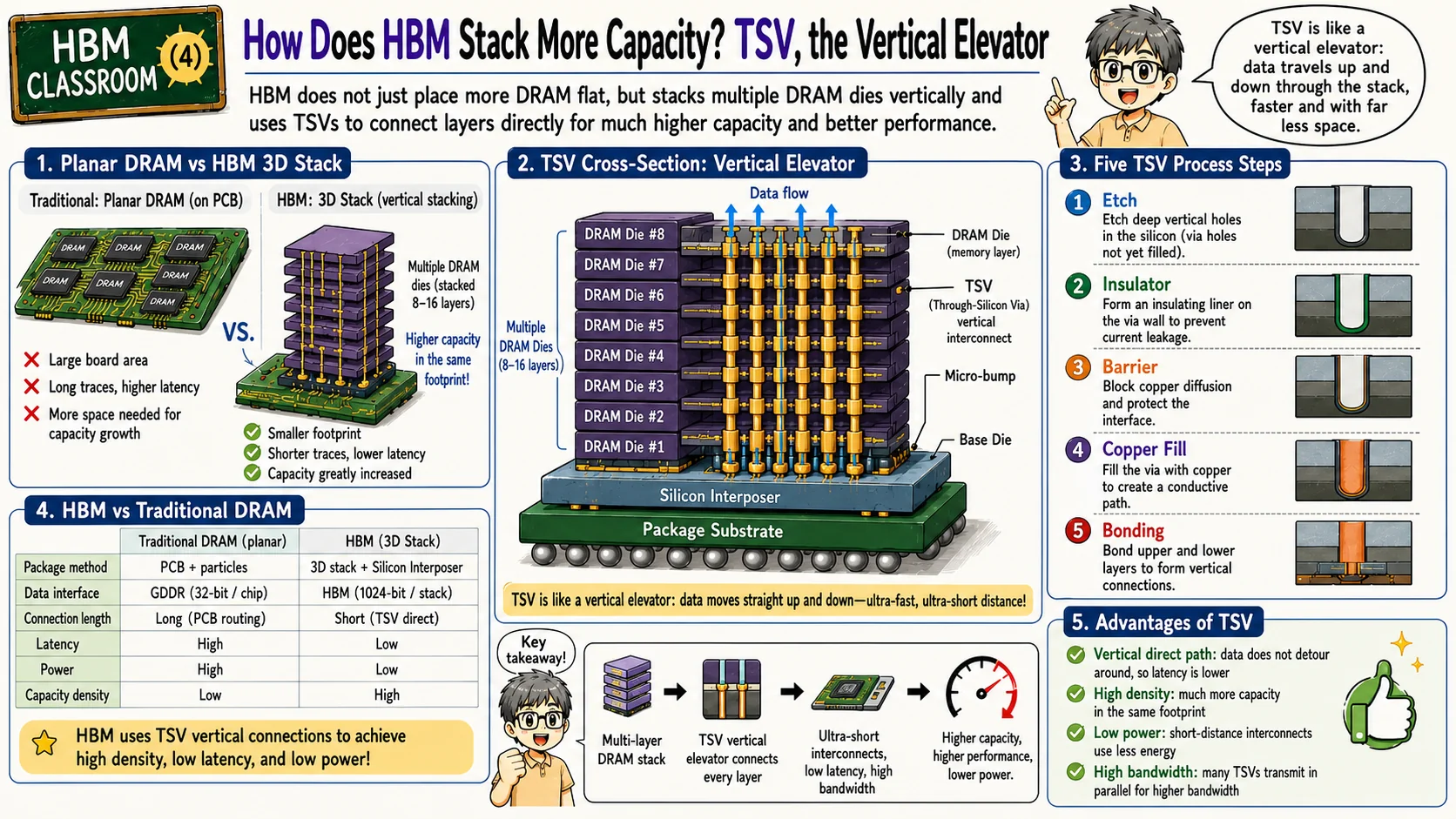
The fourth page explains how HBM gains capacity without spreading many DRAM chips across the board. Multiple DRAM dies are stacked vertically, and through-silicon vias, or TSVs, create vertical electrical paths through the silicon. The stack becomes a compact memory block with high capacity density and high bandwidth.
The elevator metaphor is useful: instead of routing data around a city, TSVs let signals move up and down through the stack. More DRAM dies can add capacity without multiplying the external data-bus width. The lab distinguishes capacity, peak bandwidth, usable bandwidth and bulk-transfer time. This shortens distance, raises density, and allows many connections to operate in parallel.
Manufacturing is the hard part. TSV processing includes etching deep vias, adding insulation liners, depositing barriers, filling with copper, planarizing, thinning, bonding, and testing. Each step can affect resistance, capacitance, leakage, mechanical stress, thermal behavior, and long-term reliability.
This is why HBM repair and base-die control matter. A practical HBM stack needs testing, training, repair paths, temperature monitoring, and control logic. The next lesson on base-die repair builds directly on this page.
HBM4 is a system challenge, not just a speed bump
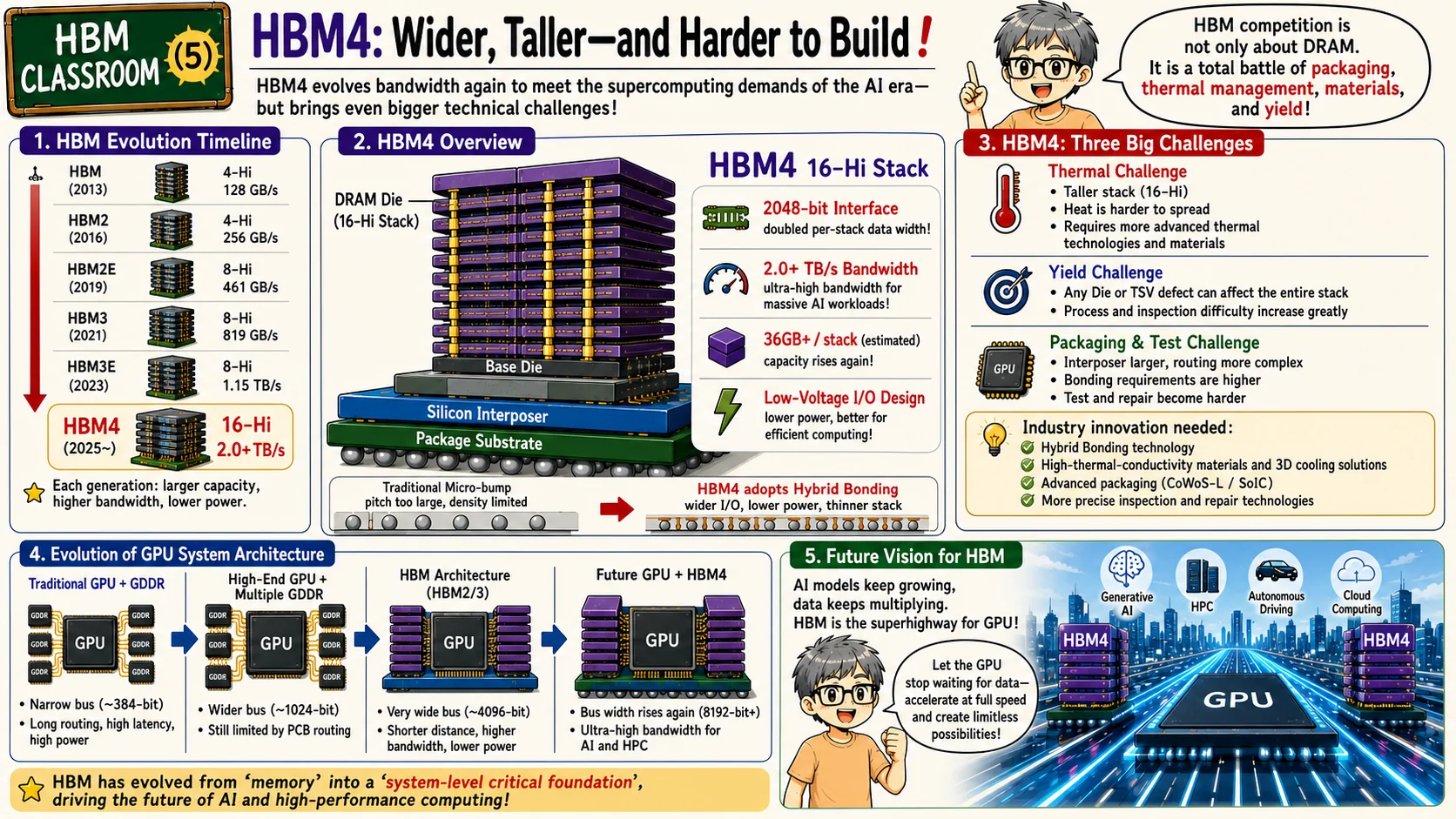
The final page points toward HBM4 and later generations. The direction is wider interfaces, taller stacks, higher per-stack bandwidth, larger capacity, lower I/O energy, and better support for AI and HPC systems. Micron’s 10 June 2025 sample announcement lists a 2048-bit interface and over 2.0 TB/s per stack; its current product page lists over 11 Gbit/s per pin and over 2.8 TB/s per stack. These are dated vendor specifications, not one guaranteed speed for every HBM4 product. Peak GB/s = data bits × per-pin Gbit/s ÷ 8.
But HBM4 is not just a faster memory chip. It raises system challenges in three areas. The first is thermal design: taller stacks and higher bandwidth make it harder to remove heat from DRAM dies, base die, interposer, substrate, and the final module. The second is yield: one die, TSV, micro-bump, or package defect can affect an expensive integrated package. The third is packaging and test: routing, bonding, inspection, repair, and known-good-stack strategy all become harder.
This is why the HBM race is not only a DRAM process race. It is also a battle of advanced packaging, materials, thermal technology, test coverage, repair architecture, and supply-chain coordination across GPU vendors, DRAM vendors, foundries, OSATs, substrate makers, equipment suppliers, and materials companies.
The final takeaway is simple: HBM makes the data path wider, shorter, and closer to the GPU. That is what lets large AI accelerators stop waiting for data and operate closer to their real compute potential.
References
- Micron HBM3E Product Page: Official HBM3E product context for capacity, bandwidth, and AI accelerator use.
- JEDEC Publishes HBM3 Update to High Bandwidth Memory Standard: JEDEC HBM3 release context for high-bandwidth memory architecture and stack capabilities.
- JEDEC Memory Standards Focus Page: Standards-family entry point for JEDEC memory technologies including HBM generations.
- TSMC 3DFabric / Advanced Packaging: Foundry-level context for CoWoS, SoIC, silicon-interposer, and 3D integration technologies.
- Micron HBM4 Shipment Announcement: Industry context for HBM4's wider interface and multi-terabyte-per-second bandwidth direction.
- Micron HBM4 current product specifications: Current vendor specifications with stated comparison conditions; not one guaranteed speed for every HBM4 product.
Exercise: separate width, data rate and capacity
Choose 1024 or 2048 data bits, then change per-pin data rate, stack count, utilization and host-path limit. Divide by eight to convert peak bits to bytes. Estimate simplified transfer time only when the working set fits.
All combinations are supplied teaching parameters, not claims that such products exist or meet JEDEC. Per-pin Gbit/s is already a data rate; do not multiply by two again for DDR. Stack traffic is assumed balanced. Refresh, command efficiency, read/write turns, power and access latency are omitted. GB/GB/s are decimal; working-set GiB is binary. More stacked dies can add capacity without automatically widening the external interface.
Learning guide
HBM and Advanced Packaging
Prerequisites
- Memory bandwidth and package basics
What I learned
- Explain why wide interfaces increase bandwidth
- Describe TSV stacking and interposers
- Identify HBM cost and integration tradeoffs