The control room sits under the stack
HBM is not just many DRAM dies stacked upward. The base die at the bottom helps the stack connect, train, test, monitor, and repair.
Traditional DRAM repair is mostly about bad rows and columns inside one die. HBM adds TSVs, micro-bumps, lanes, PHY behavior, and post-package failures, so repair becomes a 3D system problem.
Keep one idea in mind: HBM repair protects the value of the whole GPU + HBM + interposer package, not just one memory array.
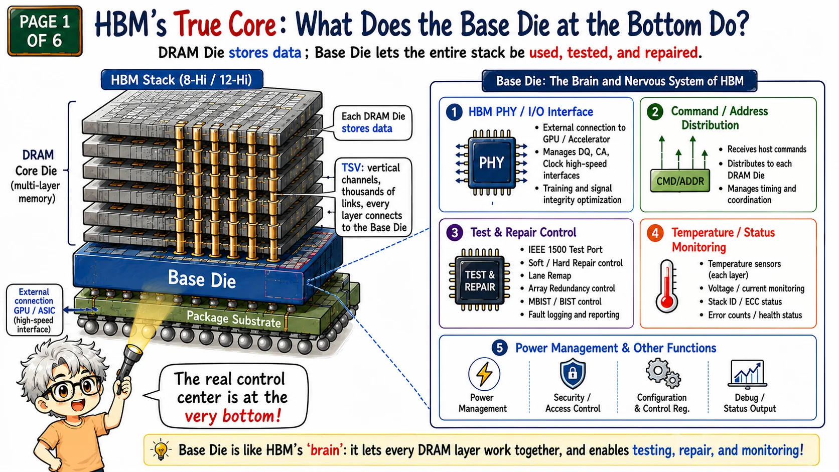
The base die is HBM's brain and nervous system
The first page explains why the base die deserves its own classroom. The upper DRAM core dies store data, but the base die is the layer that makes the stack usable by the GPU or accelerator. It connects outward to the host ASIC and upward to the DRAM dies through TSVs and micro-bumps.
Its responsibilities include HBM PHY and I/O, command and address distribution, clocking, training, calibration, test access, repair control, status reporting, temperature monitoring, power management, configuration registers, and sometimes security or access-control functions.
That makes the base die more than a passive bottom layer. It is the control plane of the HBM stack. Without it, the stack would contain memory cells, but the system would not have a practical way to coordinate high-speed access, test the vertical paths, record health data, or apply repair decisions.
For repair specifically, the base die is valuable because it can see both sides of the problem: external behavior at the GPU interface and internal behavior through the DRAM stack. That position makes it the natural place to collect fail logs, remap weak paths, manage redundancy, and improve post-assembly yield.
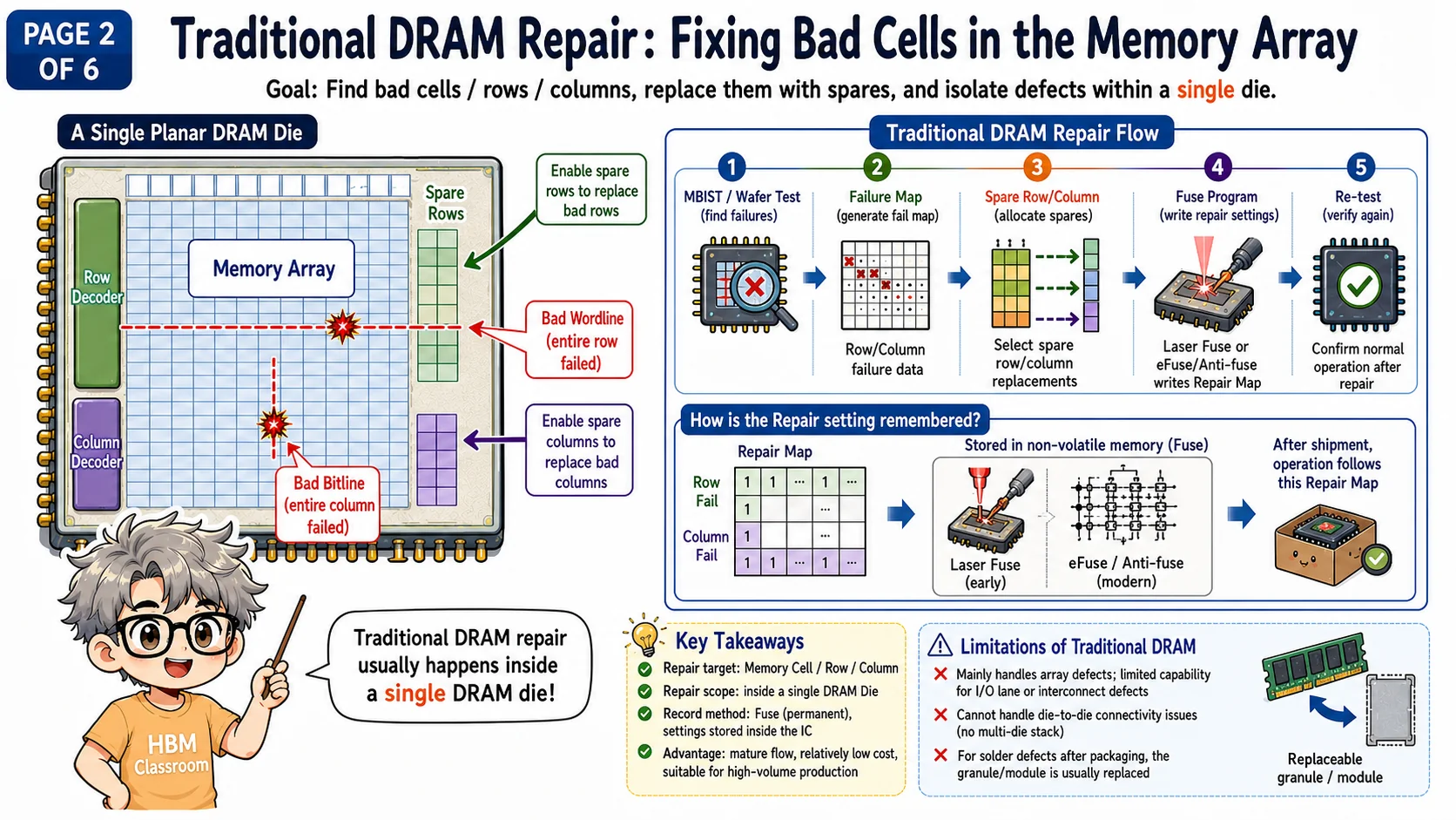
Traditional DRAM repair fixes defects inside one die
The second page establishes the baseline: classic DRAM repair mainly finds bad cells, rows, or columns inside a single planar DRAM die, then replaces them with spare rows or spare columns. The flow is mature: test, generate a failure map, allocate redundancy, program a repair map, and retest.
This works well because the repair boundary is mostly inside one die. A bad wordline can be replaced by a spare row. A bad bitline can be replaced by a spare column. The permanent repair decision can be stored in laser fuses, eFuses, anti-fuses, or other one-time-programmable elements.
The advantage is cost and maturity. High-volume DRAM manufacturing relies on this kind of redundancy to recover yield from normal array defects. After shipment, the device simply follows the stored repair map every time it powers up.
The limitation is just as important. Traditional DRAM repair does not solve die-to-die interconnect failures, TSV opens or shorts, micro-bump bonding defects, PHY lane margin problems, or post-package integration issues. HBM brings all of those into the repair conversation.
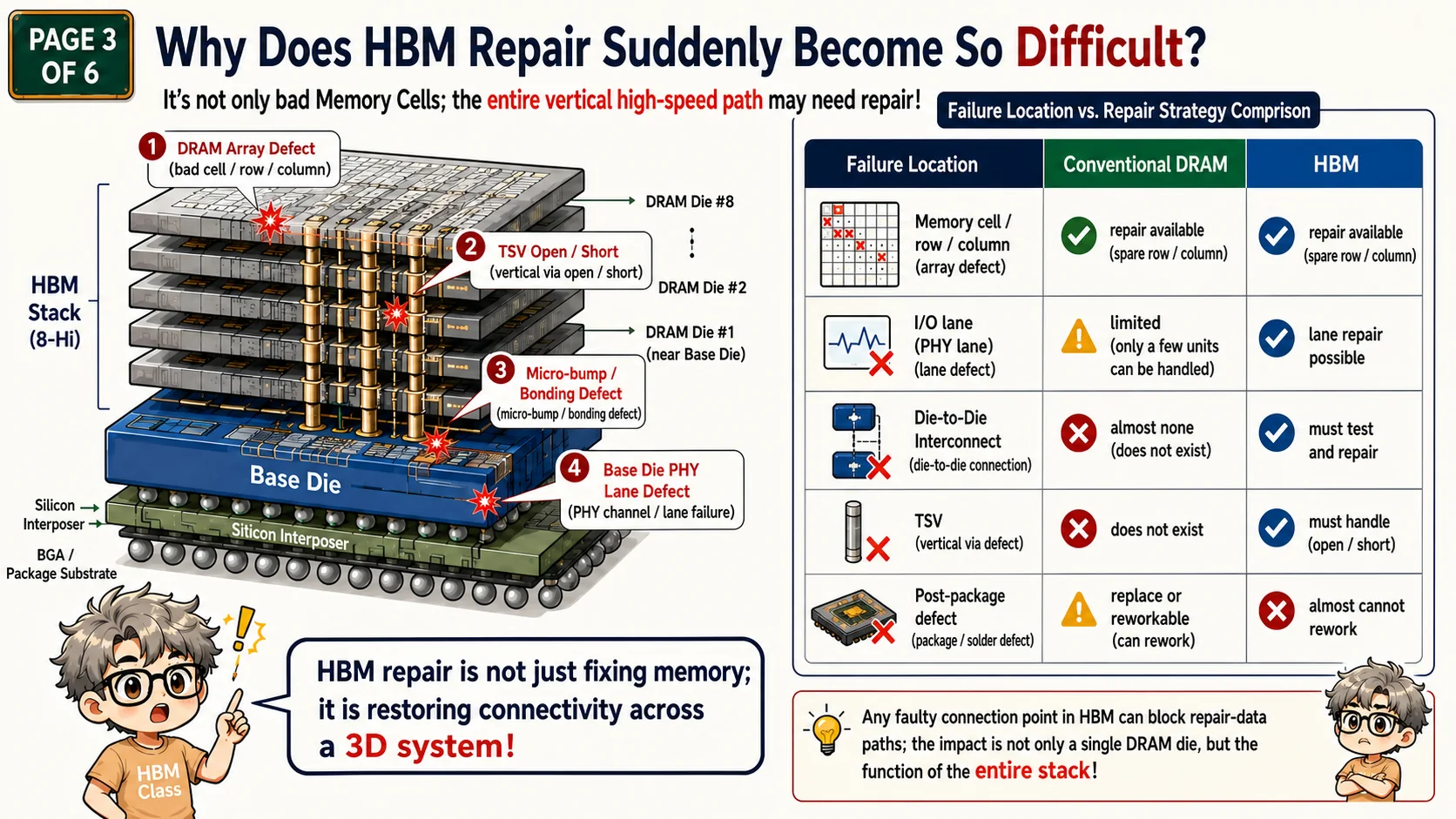
HBM repair becomes 3D system repair
The third page shows why HBM repair suddenly becomes difficult. The target is no longer only a memory array. The whole vertical high-speed path can fail: DRAM array, TSV, micro-bump, bonding interface, base-die PHY lane, interposer path, package connection, power integrity, or thermal margin.
The same user-visible symptom, such as a read error or unstable lane, may have several root causes. It could be a bad memory cell, a weak TSV, a marginal micro-bump, a timing issue in a lane, or a stress-sensitive connection that only appears after stacking and packaging.
That is why HBM repair needs failure classification. Array defects can use spare rows or columns. Lane defects may need lane remapping. TSV or link defects may require avoiding a bad vertical path. Package-level defects may not be reworkable, so they must be handled by built-in redundancy or caught earlier in the test flow.
In other words, HBM repair is connectivity repair across a 3D system. The goal is not only to save memory capacity; it is to keep the whole stack electrically usable, trainable, and reliable after integration.
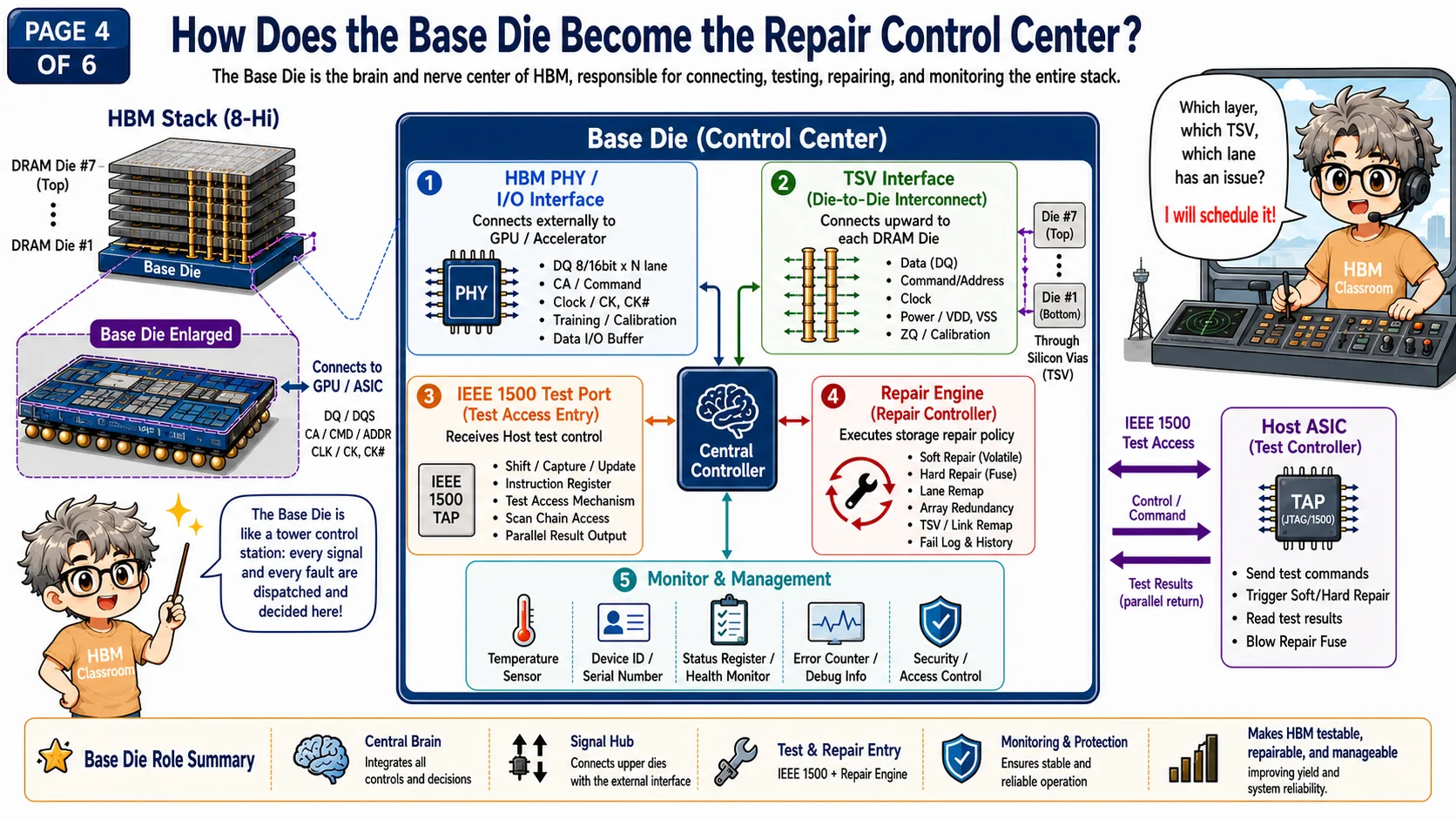
The base die becomes the repair control center
The fourth page zooms into the repair-control architecture. The base die sits at the bottom of the stack, so it is naturally connected to the outside world through the HBM PHY and to the upper DRAM dies through TSV interfaces. That makes it the right place to coordinate test, diagnosis, remapping, monitoring, and final repair programming.
A practical base-die control center includes several blocks. The PHY and I/O interface manage external data, command, clock, and training. The TSV interface reaches the stacked dies. The IEEE 1500 test port or a related test-access structure lets a host tester shift commands, capture results, update instructions, and observe internal states.
The conceptual repair block collects soft/hard mapping, lane/link remapping, array redundancy and logs. Actual placement across base die, core dies and external testers varies by product; this is not a mandatory block list for every HBM device. Monitoring logic adds temperature sensors, status registers, error counters, device identity, debug output, and health indicators.
The point is observability plus action. A stack cannot be repaired well if the system cannot identify which layer, TSV, lane, or array region failed. The base die turns scattered failures into manageable repair decisions.
Soft repair validates; hard repair makes it permanent
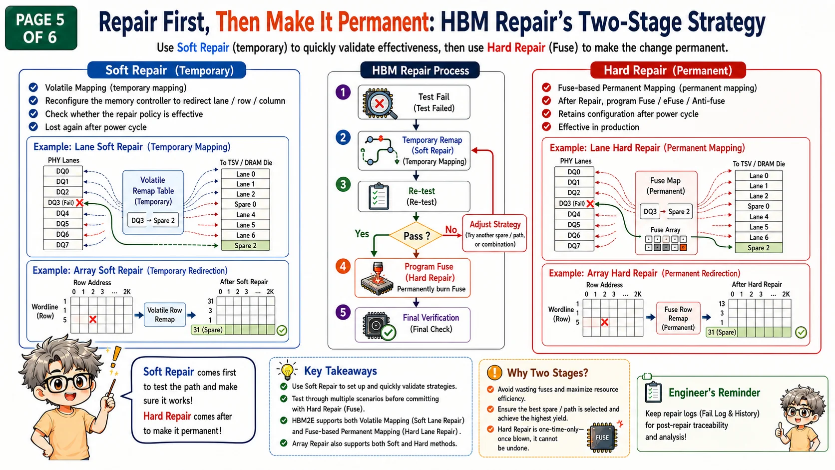
The fifth page explains the two-stage strategy. Soft repair uses volatile mapping, registers, or temporary configuration to try a repair choice before permanently committing it. Engineers can redirect a lane, row, column, or spare path, then retest to see whether the margin and behavior improve.
Soft repair matters because the best repair choice is not always obvious at the first failure. Different stages, wafer test, stack test, package test, and system bring-up, can reveal different limitations. Temporary mapping lets the team compare options before using one-time resources.
Hard repair comes after validation. Once a repair strategy passes the required tests, the final map can be programmed into fuse, eFuse, anti-fuse, or another non-volatile repair element. The repaired configuration then survives power cycles and becomes the production state.
Temporary mapping permits testing before a permanent record is committed. A strong flow checks that the failure type is supported, healthy spares remain and retesting passes before permanent programming. The experiment writes and reads patterns on eight synthetic lanes; it refuses a hard-map commit after a failed retest and loses the temporary map on reboot. Test payload is freshly written after reboot, not retained by DRAM without power.
Post-packaging repair protects the whole AI package
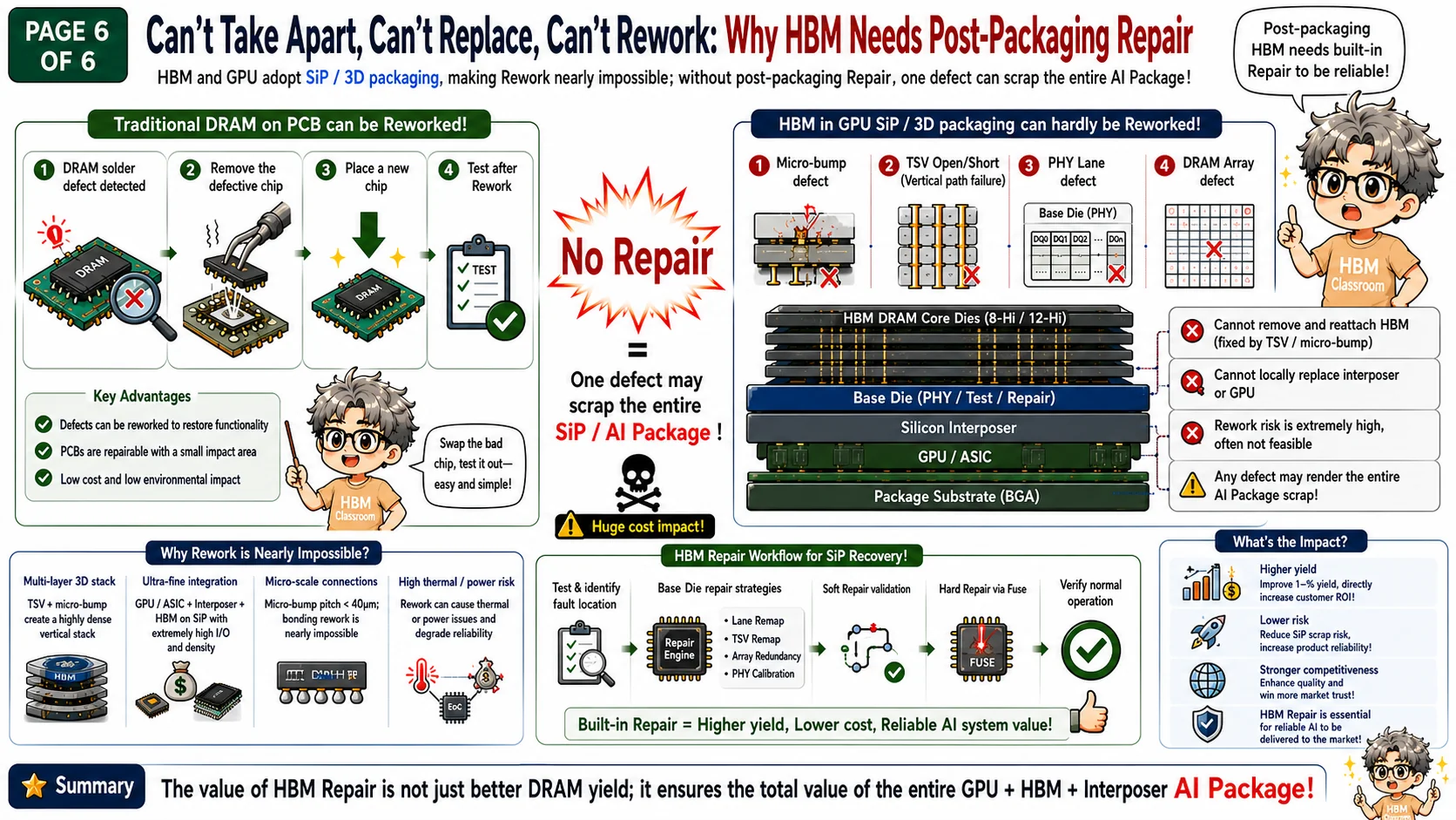
The final page shifts the economic boundary from memory yield to package yield. Traditional DRAM on a PCB can sometimes be replaced or reworked. HBM inside a SiP, 2.5D, or 3D AI package is very different. The HBM stack, GPU or ASIC, silicon interposer, micro-bumps, and package substrate are tightly integrated, and rework is often impractical or too risky.
That means a small defect can destroy a large amount of value. A micro-bump defect, TSV open or short, PHY lane failure, or late-appearing DRAM array defect may threaten the entire GPU plus HBM plus interposer package if there is no built-in repair path.
Post-packaging repair therefore protects more than DRAM bits. It protects effective yield, reduces scrap risk, improves reliability, and can directly affect the supply and cost of high-end AI accelerators. Even a modest yield recovery can matter when each package contains expensive compute silicon and multiple HBM stacks.
The final takeaway is that HBM repair is infrastructure. The base die, repair engine, test access, telemetry, soft repair, hard repair, and post-package recovery flow all work together to make the final AI package manufacturable, testable, and reliable.
References
- Micron HBM2E Memory White Paper: Official HBM2E architecture background including stack organization, channels, soft lane repair, and hard lane repair.
- IEEE 1500-2025 Standard Page: Embedded-core test access and wrapper standard relevant to test control in complex stacked devices.
- SemiEngineering: HBM Shifts Testing Left To Preserve AI Chip Yield: Industry context for HBM testing, yield preservation, packaging cost, and AI package economics.
- SK hynix Hot Chips Tutorial: High Bandwidth Memory: Technical background on HBM stack organization, base die, TSVs, interposer integration, and system architecture.
- Micron HBM3E Product Page: Official product context for modern HBM bandwidth, capacity, and AI accelerator use.
Exercise: temporary mapping, verification, permanent record and reboot
Eight logical lanes write and read known patterns. Redirect failed lanes to healthy spares and retest. Only a passing map may be saved to a simulated permanent record. Reboot loses the soft map, showing what the hard map provides.
Eight lanes, two spares and pattern memory form a custom model, not an HBM repair protocol, IEEE 1500 implementation or real fuse operation. Only independent data-lane faults are modeled; arrays, command, clock, shorts and correlated failures require separate analysis. Test data is freshly written after reboot; no DRAM power-off retention is claimed. Healthy spares and test coverage are supplied assumptions, not recovery from every package defect.
Learning guide
HBM and Advanced Packaging
Prerequisites
- HBM stack and TSV organization
What I learned
- Explain the base die control role
- Compare array repair with lane and stack repair
- Understand post-package repair needs