Advanced packaging moves chips closer together
AI systems are not limited only by what one die can compute. They are also limited by how quickly data can move between GPU, HBM, interposer, substrate, and board.
The plates separate the layers: CoWoS, silicon interposer, CoPoS, ABF substrate, and PCB. Each layer solves a different distance, density, routing, or reliability problem.
Read it as a data-road story: packaging tries to make the road shorter, wider, and reliable enough without breaking cost, yield, or thermal limits.
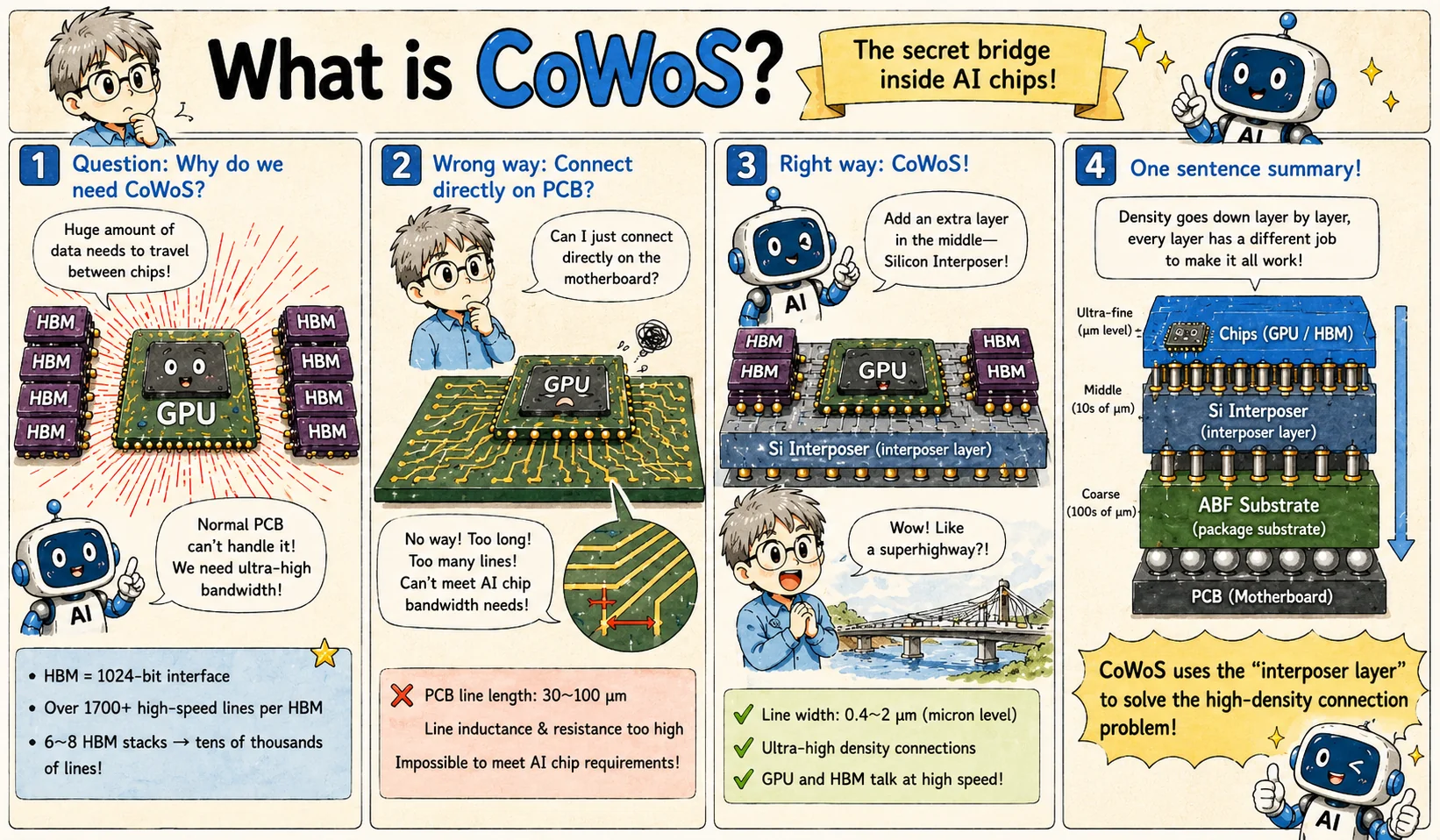
CoWoS solves the chip-to-chip bandwidth problem
The first page starts from the central problem: AI accelerators need enormous memory bandwidth between the compute die and nearby HBM stacks. That traffic is not a vague software flow. It is thousands of short, high-speed electrical connections that must fit into a very small physical area.
A normal PCB is too coarse for this job. Its traces are longer, wider, and less dense, which increases signal loss, parasitics, latency, and routing congestion. The illustrated CoWoS-S design inserts a silicon interposer between the chips and the package substrate so GPU and HBM can communicate through very dense, short, clean routes.
This is why CoWoS became important for AI. It is not only a packaging brand name; it is a system architecture choice that makes high-bandwidth logic-plus-memory integration practical.
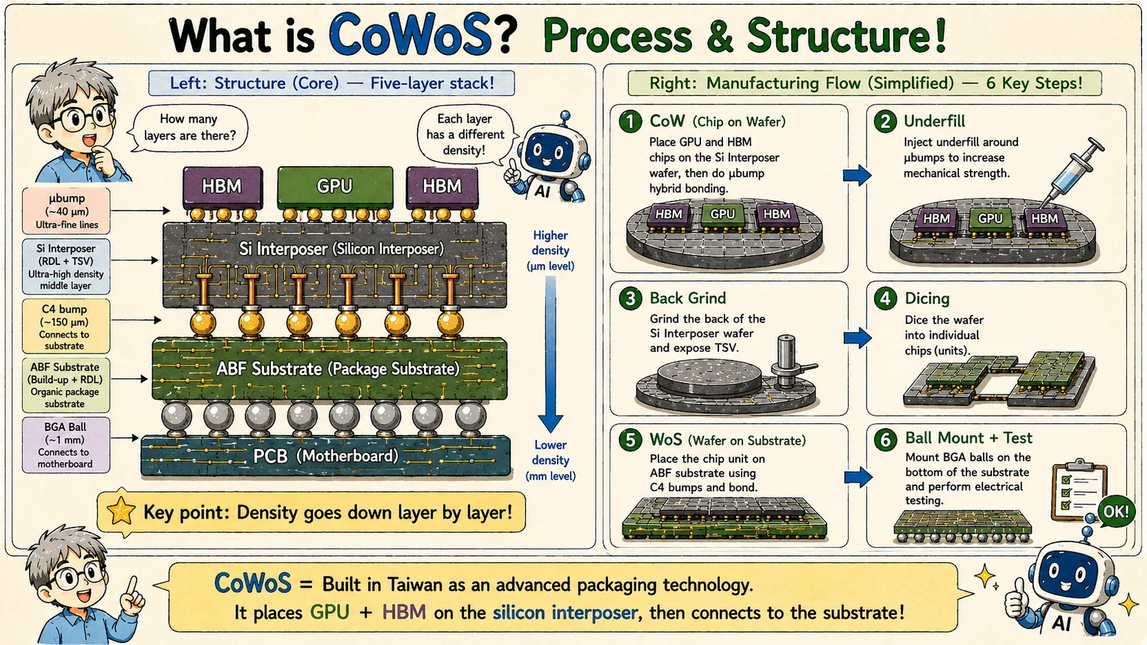
CoWoS process and stack structure
The second page separates the structure from the process. This illustration follows a CoWoS-S-style silicon-interposer stack, not every CoWoS variant. TSMC also lists CoWoS-R with polymer/copper RDL and CoWoS-L with RDL plus local silicon interconnect. The illustrated connection-density levels are: GPU and HBM on top, microbumps into the silicon interposer, C4 bumps into the ABF substrate, BGA balls into the motherboard, and finally the broader system PCB.
The manufacturing flow is also staged. Dies are placed on the silicon interposer wafer, underfill is added for mechanical strength, the wafer is thinned and diced, the unit is attached to the substrate, and then balls are mounted and tested. Each step has yield, warpage, thermal, and reliability implications.
The key lesson is that bandwidth is physical. You cannot get unlimited data movement by naming a faster interface. The package must provide enough parallel wires, short enough routes, clean enough signals, and a mechanical stack that survives assembly and operation.
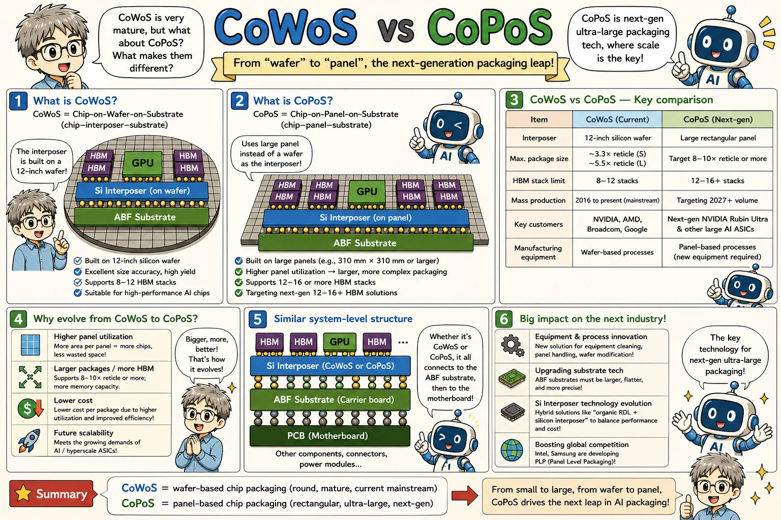
CoPoS extends CoWoS thinking from wafer to panel
The third page compares CoWoS and CoPoS. CoWoS is wafer-based and already mature in high-end AI packaging. CoPoS pushes the same idea toward large rectangular panels, aiming for larger package area, more HBM stacks, and better area utilization for very large accelerator modules.
That shift sounds simple, but it changes the manufacturing problem. Panel-level packaging needs new equipment, cleaning, alignment, bonding, warpage control, metrology, and yield learning. The larger the panel and package become, the more mechanical and process variation matters.
So CoPoS is best understood as a scaling direction, not merely a new acronym. It tries to keep the same system-level idea: dense chip-to-chip interconnect above a substrate, but at a larger manufacturing scale.
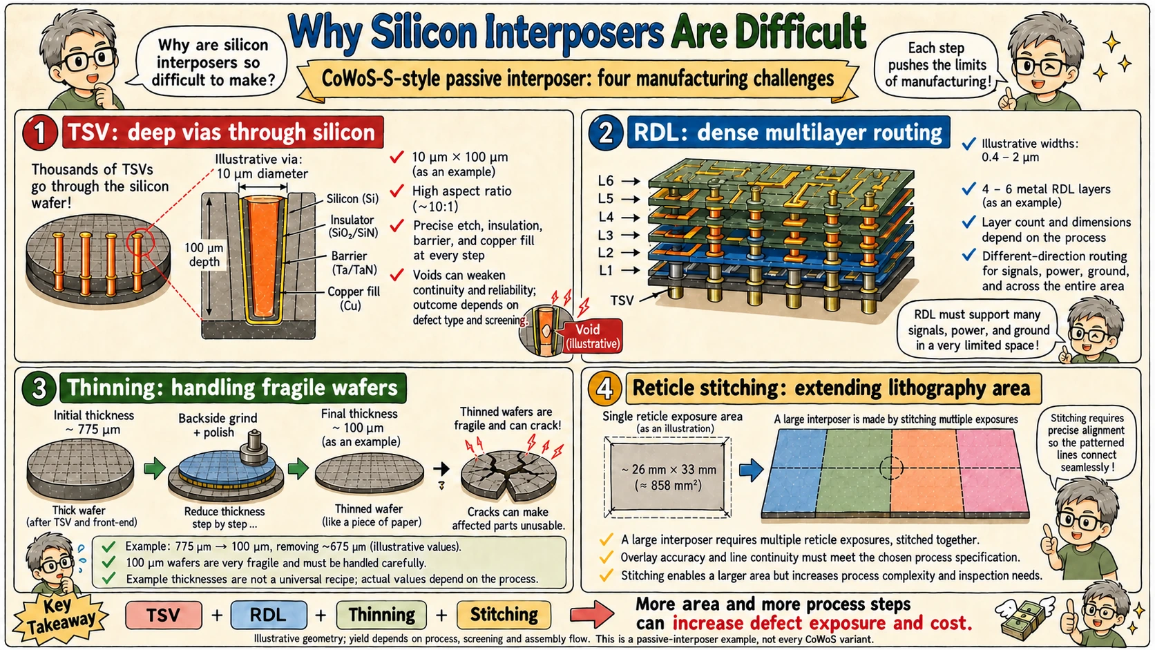
A silicon interposer is manufactured like a wafer-level routing chip
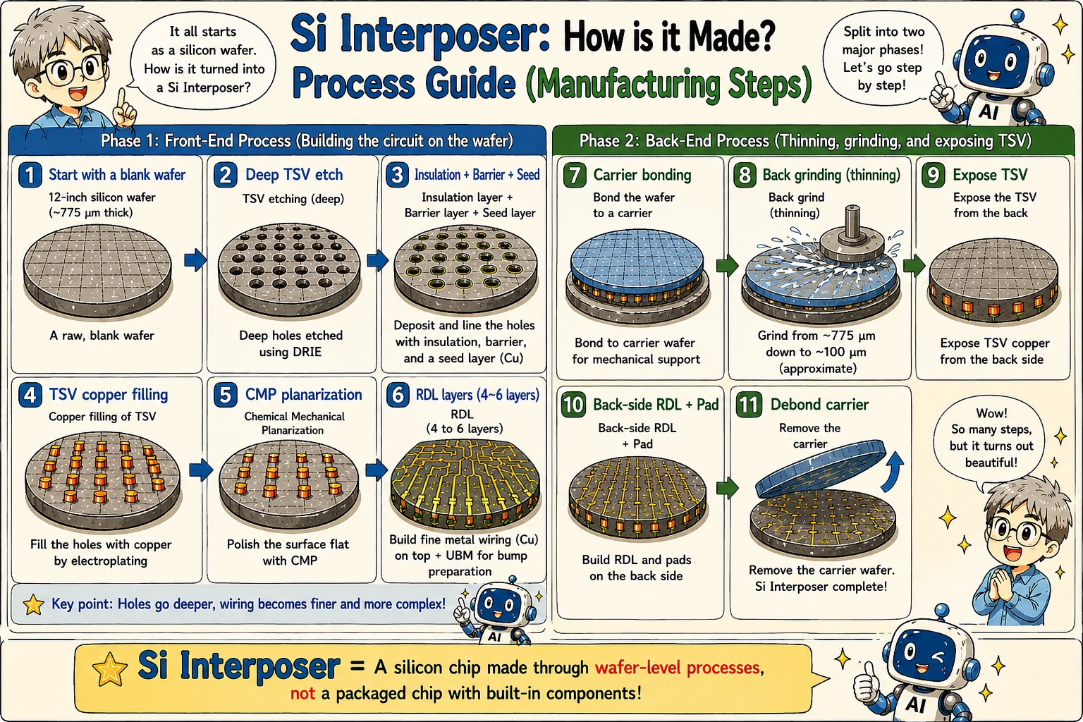
The fourth page zooms into silicon interposer manufacturing. This lesson illustrates a passive silicon interposer used mainly for routing; passive does not mean electrically empty. Active interposer designs also exist, so this example does not define every implementation. It begins as a silicon wafer and is processed into a high-density routing layer using wafer-level steps such as deep TSV etch, insulation, barrier and seed deposition, copper filling, CMP, and RDL formation.
The back-end sequence is just as important: carrier bonding, back grinding, TSV exposure, backside RDL and pad formation, and carrier debonding. These steps create both lateral routing and vertical connections so signals can travel from the top dies down to the substrate.
This explains both the power and the cost of silicon interposers. They can route far more densely than organic substrates, but they inherit semiconductor-style process complexity, capacity constraints, and yield sensitivity.
Interposer density is the hidden bridge
The fifth page reinforces the density hierarchy. At the top, GPU and HBM use very fine microbump-level connections. The silicon interposer provides micron-level routing with RDL and TSVs. Below that, the ABF substrate fans signals and power outward. The PCB then connects the package to the server system.
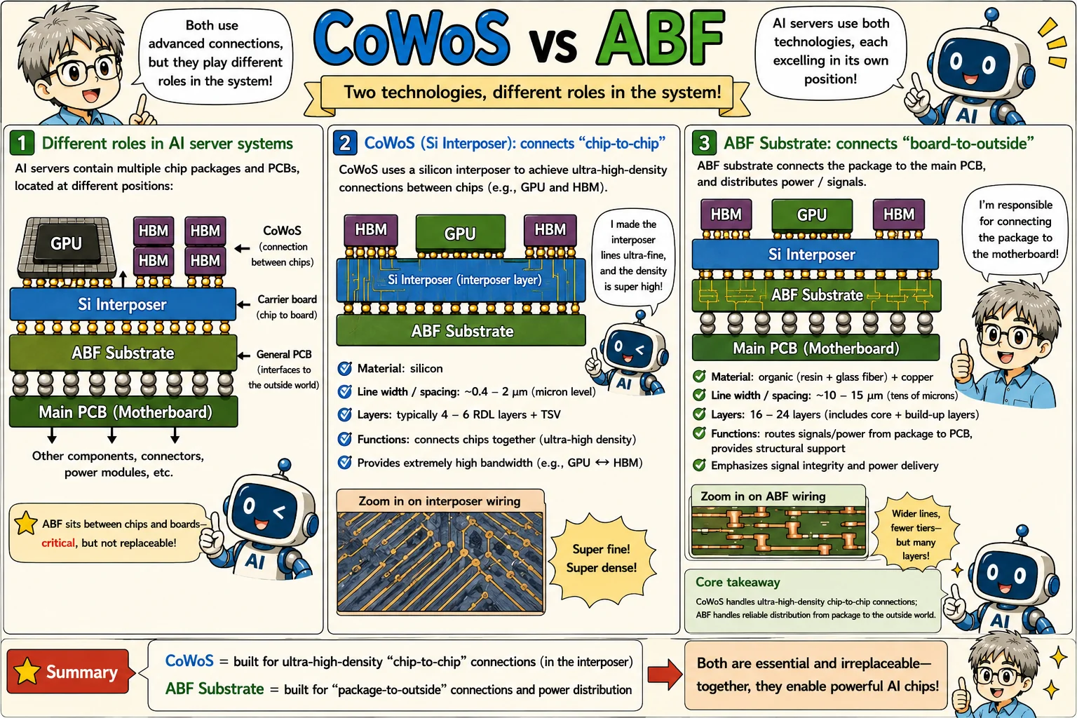
This hierarchy matters because every layer has a different job. The interposer is optimized for short, dense, chip-to-chip communication. The ABF substrate is optimized for package support, fanout, power delivery, and board attachment. The PCB is optimized for system-level connectivity.
A useful mental model is: density decreases as the signal moves away from the die. If you ask a coarse layer to do the job of a fine layer, the system runs into pitch, signal-integrity, parasitic, and routing limits.
CoWoS and ABF are complementary, not substitutes
The sixth page fixes a common misunderstanding: CoWoS and ABF are not competing answers to the same question. The illustrated CoWoS-S design uses the silicon interposer for ultra-high-density chip-to-chip connections. ABF is a build-up dielectric film; a substrate using it provides package-to-board fanout, power distribution and structural support. The material name and the completed substrate are different concepts.
An AI server package typically needs both. The GPU/HBM side needs the interposer's fine routing density. The package also needs the ABF substrate to connect that dense internal world to the motherboard through larger bumps, wider routing, and robust mechanical support.
This is why advanced packaging supply chains can have more than one bottleneck. Interposer capacity, ABF substrate capacity, assembly, test, HBM supply, thermal solution, and substrate qualification can all limit the number of finished accelerator modules.
ABF is not a normal PCB
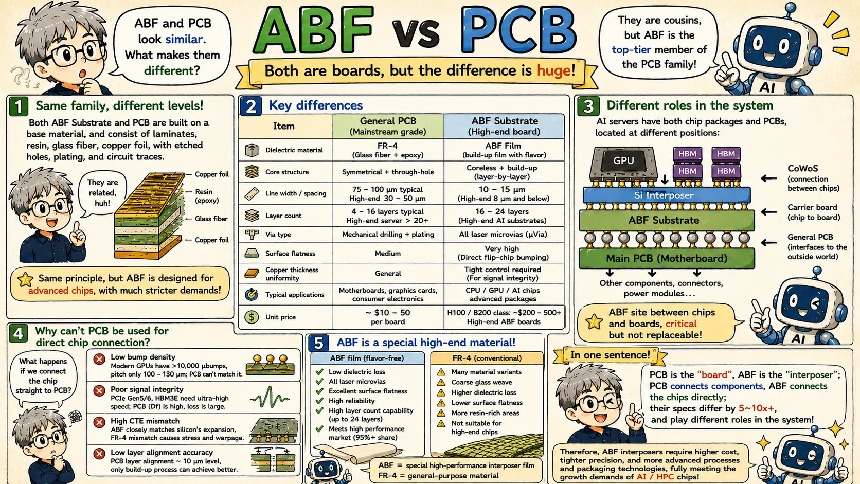
The final page compares ABF substrate with ordinary PCB. They are related in the broad sense that both are laminated boards with dielectric materials, copper wiring, vias, and layers. But their precision class and system role are very different.
ABF substrates must support high I/O density, fine-pitch flip-chip bumps, tight layer alignment, copper uniformity, flatness, warpage control, CTE compatibility, and package-level reliability. Ordinary PCBs are designed for broader system interconnect and cannot directly replace this role in GPU/HBM packages.
For engineers, the takeaway is that advanced packaging is architecture. CoWoS, silicon interposers, ABF substrates, PCBs, HBM, and chiplets are not isolated manufacturing terms. They are the physical constraints that determine bandwidth, cost, yield, power delivery, thermal behavior, and product feasibility.
References
- TSMC 3DFabric advanced packaging: Official overview of TSMC's 3DFabric family, including CoWoS, SoIC, and InFO.
- TSMC CoWoS: Official CoWoS reference for chip-on-wafer-on-substrate integration and high-density HBM packaging.
- ASE 2.5D and 3D IC packaging: Industry overview of 2.5D/3D packaging, HBM integration, and heterogeneous integration platforms.
- Ajinomoto Build-up Film: Official Ajinomoto reference on ABF material used in high-performance semiconductor package substrates.
Exercise: tracks must fit in the correct layer
Choose the connection level, then change available width and signal count. Calculate floor(width/pitch) and check both role and capacity. Then see how independent yields multiply for multiple unscreened dies.
The supplied 2/20/100 μm pitches are classroom rules, not CoWoS/ABF/PCB design rules. Only single-layer parallel signal tracks are counted; power, clock, vias, keepouts, signal integrity, thermal constraints and DRC are omitted. No real package is designed. Yield assumes unscreened dies and independent failures; it cannot be applied to known-good-die supply or correlated defects. Not every CoWoS variant uses a full silicon interposer.
Learning guide
HBM and Advanced Packaging
Prerequisites
- Basic chip, package, and PCB concepts
What I learned
- Separate interposer, substrate, and PCB roles
- Explain why chiplets need dense integration
- Recognize ABF substrate constraints