Start with the distance data must travel
Imagine a school where every classroom sends each worksheet to a warehouse across town. Faster students still wait for the truck. AI accelerators face a similar problem when weights and activations repeatedly cross memory and chip boundaries.
These twelve plates follow one route: keep the wafer intact, stitch exposure fields, route around defects, place SRAM beside small cores, move data across a 2D mesh, and let software map the model.
Read the visual story first. Then open the engineer notes for physical design, distributed memory, network traffic, model residency, benchmark boundaries, and prefill/decode behavior.

Why does AI often stall while moving data?
Picture an AI system as a school campus. Classrooms do the math, whiteboards hold nearby notes, and roads carry information from one room to the next. Even brilliant students must wait if the right books have not arrived.
Four measurements tell different stories. Compute is how many problems the students can solve. Capacity is how many books the rooms can hold. Bandwidth is how many trucks can use a road at once. Latency is how long the first truck takes to arrive. A wide road is not automatically a short trip.
Some workloads are compute-bound: they truly need more arithmetic. Others are movement-bound: the arithmetic units spend time waiting for weights, activations, gradients, optimizer state, or KV cache. The bottleneck changes with training versus inference, model shape, batch size, and placement.
Crossing a chip, package, board, or rack boundary can add links, protocols, energy, and scheduling. Cerebras puts many small processors, distributed SRAM, and an interconnect on one wafer to shorten some of those trips. [1]
Host I/O, storage, and networking still exist. The useful questions are therefore concrete: what is moving, where did it start, which boundaries disappeared, and did the saved waiting time outweigh the new system costs?
Why leave the wafer uncut?
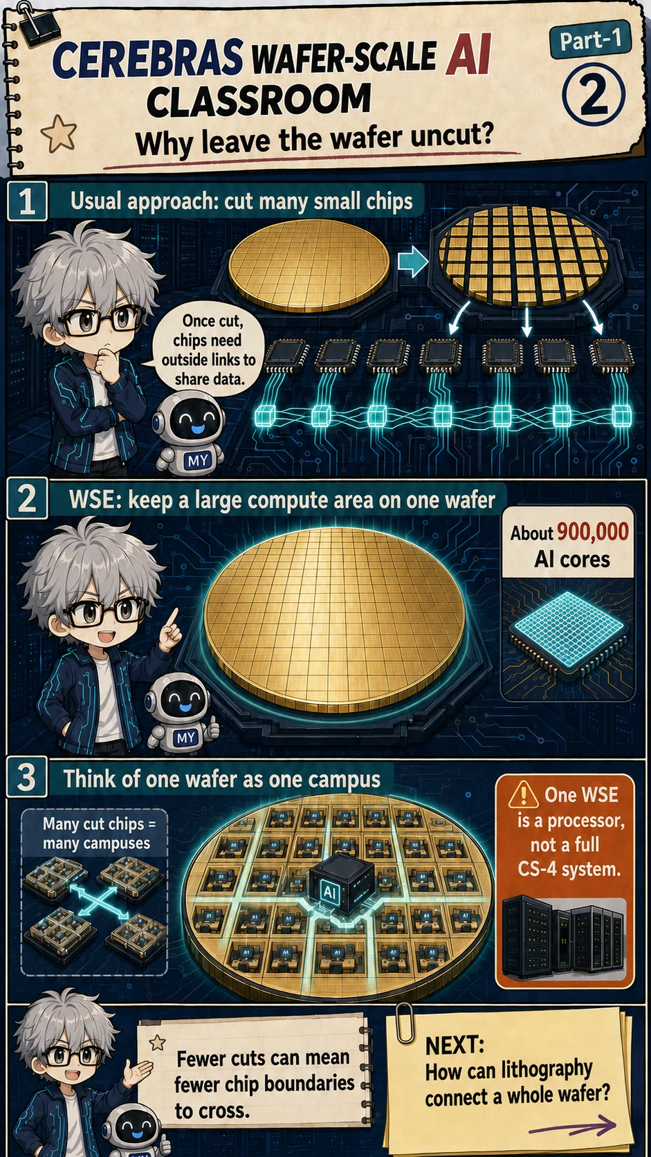
A normal wafer is cut into separate dies. Each die goes into a package and onto a board; larger systems may then connect accelerators, servers, and racks. Those boundaries make products easier to assemble and replace, but data has farther to travel.
The Wafer-Scale Engine leaves its main compute area uncut, so many cores communicate across one piece of silicon. It removes some die-to-die and package-to-package journeys. It does not squeeze an entire data center onto one wafer.
WSE-3T is the engine, not the whole machine. Cerebras lists one wafer at 46,225 mm², four trillion transistors, about 900,000 AI cores, and 44 GB of on-chip SRAM. [1]
CS-4 is the deployable system. It combines three WSE-3T processors with power, liquid cooling, control, and I/O. When reading a specification, first check whether the number describes one wafer or the complete system. [2]
Keeping the wafer whole removes communication borders but creates hard manufacturing, testing, power, cooling, and service problems. The Cerebras design is a chip, package, system, and software project taken together—not simply an oversized die.
How do you build beyond one reticle field?
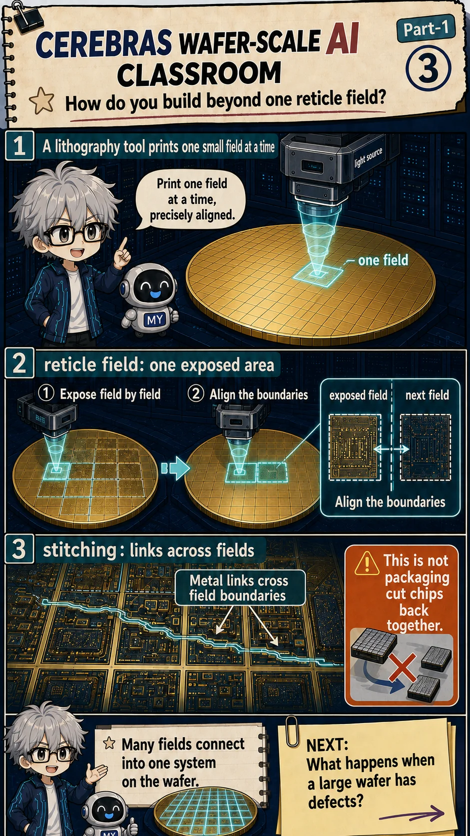
A chip pattern is not printed across the whole wafer in one shot. A mask carries the circuit pattern, and a step-and-scan tool exposes one fixed-size area at a time. That area is a reticle field.
Most chips stay inside one field and are cut out as separate dies. A wafer-scale design must cross that size limit by making metal wires meet accurately at neighboring field boundaries.
That boundary connection is reticle stitching. The comic shows neat floor tiles, but the real job is to align electrical paths while accounting for process variation and placement error.
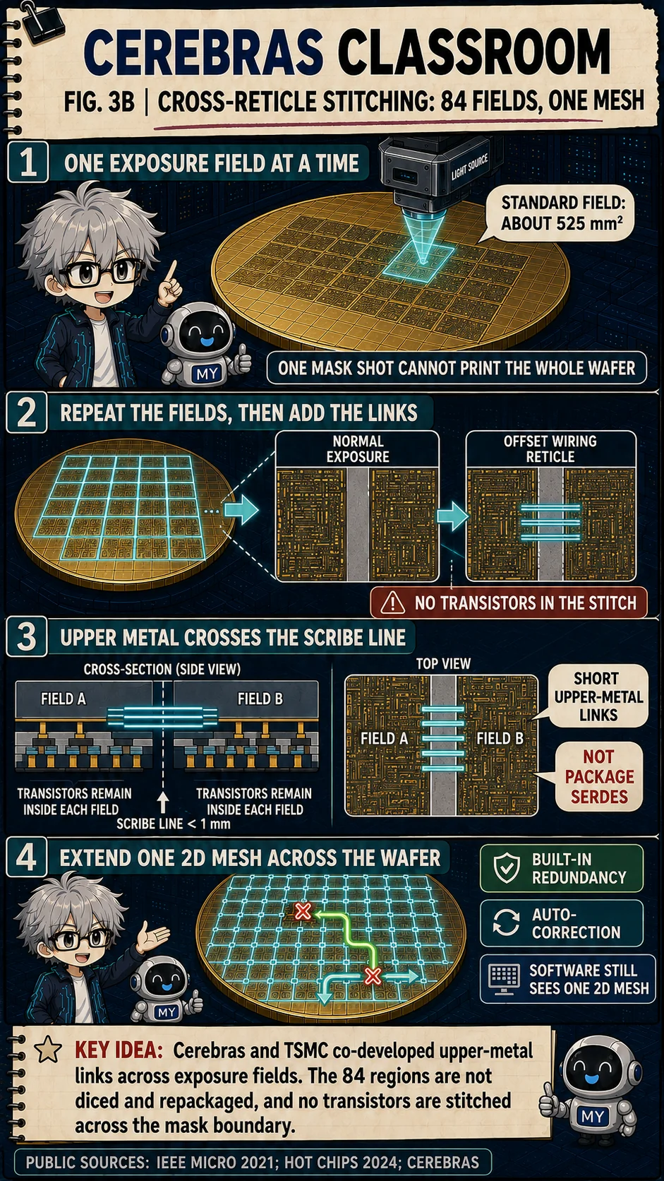
The published IEEE Micro account gives a more concrete sequence. WSE-2 first used a conventional step-and-repeat reticle of about 525 mm². A second, offset wiring reticle then exposed the joins between neighboring fields. Those extra shots made upper-level interconnect metal only—not transistors or other active circuitry. [7]
Cerebras adds the electrical view: the links cross less than one millimeter of scribe line in high-level metal within the TSMC process. Short parallel, source-synchronous interfaces extend the on-die 2D mesh, and more than a million cross-boundary wires add up across the wafer, so the protocol includes training and auto-correction. [8]
At Hot Chips 2024, Cerebras showed WSE-3 as 84 die regions joined into one fabric and said the cross-boundary process was extended to 5 nm in collaboration with TSMC. Here, '84 dies' means reticle-sized design regions left together on one uncut wafer—not 84 packaged chiplets connected through package SERDES. [9]
Stitching does not require a physically perfect wafer. Built-in fabric redundancy can disable a failed core or link and route around it, while software still sees a regular 2D mesh. Stitching answers how fields connect; redundancy answers how the machine keeps working when part of that fabric is defective. [9]
Stitching and chiplets connect things at different stages. Stitching joins exposure fields while the wafer remains whole. Chiplets connect already separate dies through advanced packaging. The distance, density, testing, and repair choices are different.
Crossing a field is only the first test. Timing, power delivery, test access, and multilayer routing must still work across the full wafer, so 'connected' also has to mean reliable and on time.
Engineer extension: stitching is a physical-design contract
Cross-reticle links must be planned across exposure boundaries with alignment tolerance, metal routing, clock and power distribution, timing closure, test access, and yield strategy. The field grid is regular, but it does not turn physical closure into a copy-and-paste problem.
How can a wafer work with defects?
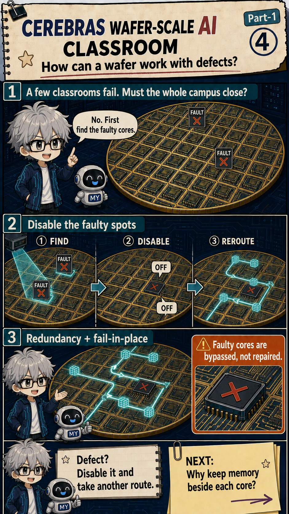
A huge silicon area is unlikely to be perfect everywhere. If one bad core ruined the whole wafer, a wafer-scale processor would be extremely difficult to ship in useful numbers.
The number of defects is not the entire story. Ten scattered defects may be easy to route around, while ten defects clustered near a critical corridor may isolate a much larger region. Distribution and remaining connectivity matter.
The response follows four steps: test the wafer, disable bad regions, enable reserved resources, and reroute traffic. Cerebras describes redundant compute, redundant routing, and fail-in-place. The broken transistors are bypassed, not repaired. In the experiment below, disable a tile and follow each hop through a 4×4 grid. Cutting a full column can disconnect its two sides. The custom BFS/store-and-forward model checks reachability; it does not simulate WSE routing, clock timing or yield. [1]
Testing produces a map of usable resources. System configuration and compilation can then avoid failed processing elements and links, placing work only in regions that still form a connected fabric.
Spare resources, testing, binning, and remapping all cost area and effort. The engineering target is not a physically flawless wafer; it is a predictable, verifiable product despite a reasonable defect pattern.
Engineer extension: yield comes from architecture plus test
Redundant cores and routes only help when manufacturing test can identify unusable resources and the configuration flow can create a valid connected fabric. Spare ratio, defect clustering, routing reachability, and performance binning belong to the same yield model.
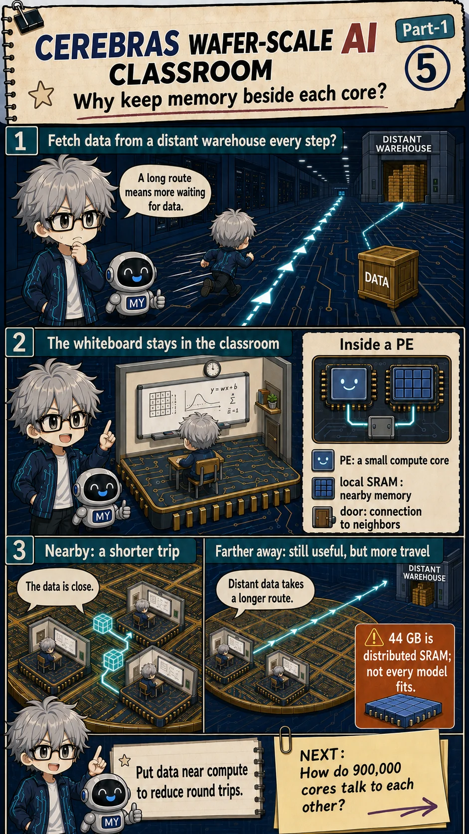
Why keep memory beside each core?
A processing element, or PE, is like one student desk with three parts: a worker that computes, a whiteboard for nearby notes, and doors leading north, south, east, and west. In hardware, those parts are a compute engine, local memory, and a router connected to the 2D mesh. [3]
SRAM is the desk-side whiteboard: fast and nearby, but expensive in silicon area per stored bit. HBM or ordinary DRAM is more like a larger library. It can hold more, but data must cross a longer interface and path to reach compute.
Keeping frequently used data in local SRAM can save time and energy. Each PE, however, directly owns its local data and code; another PE cannot treat it as one transparent shared whiteboard. [3]
The WSE-3T's 44 GB is the total SRAM distributed across the wafer. The compiler must decide where data lives, whether it is copied, when it moves to a neighbor, and when its space can be reused. [1]
Poor placement can send data on long routes, crowd a few links, or leave compute idle because one PE ran out of room. Nearby memory is an opportunity created by hardware; software still has to capture that locality.
Engineer extension: distributed SRAM changes the programming model
Local PE memory is not a hardware-coherent global address space. Placement, replication, streaming, and explicit communication determine whether locality is achieved. Capacity numbers should therefore be paired with mapping efficiency and the working set of each phase.
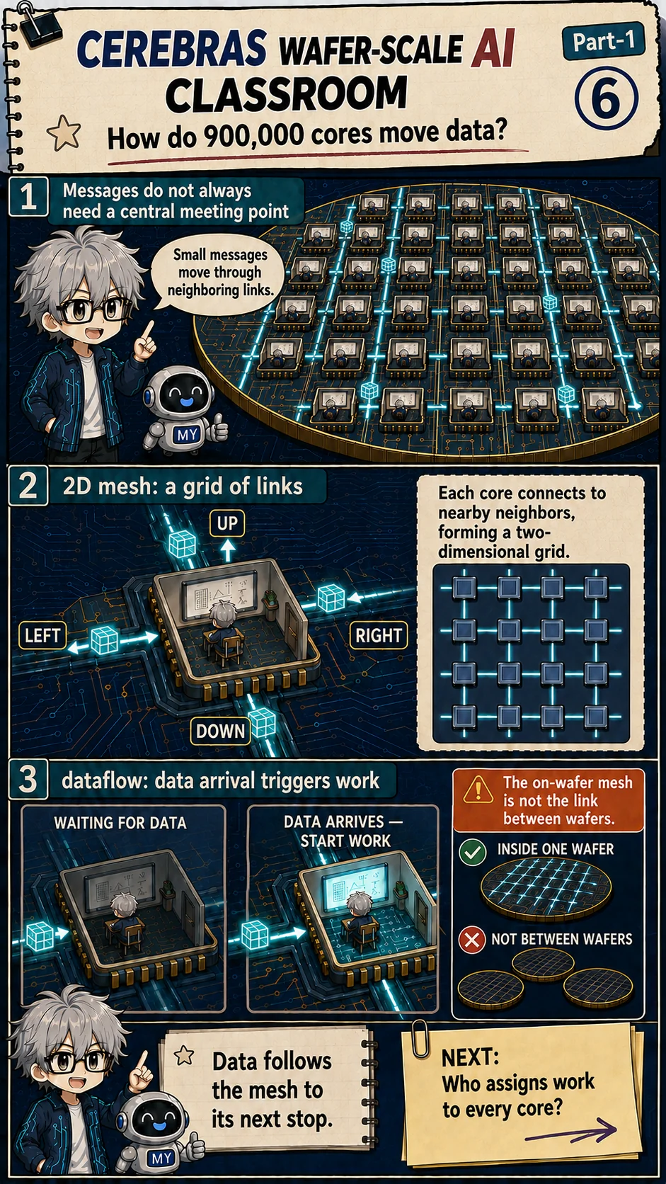
How do 900,000 cores move data?
If every classroom exchanged papers through one central office, that office would become a traffic jam. Each WSE router instead connects to its north, south, east, and west neighbors, creating many paths across a two-dimensional mesh. [3]
Every router crossed is one hop. Nearby exchanges take few hops; distant destinations take more. Routing chooses the path, while placement determines how far apart the sender and receiver were in the first place.
When many flows want the same link, they contend. If the next stop cannot accept data quickly enough, pressure can travel backward. A mesh does not abolish congestion; it gives software many distributed paths instead of one central choke point.
The Cerebras SDK calls each small 32-bit message a wavelet. When data arrives at a PE, it can activate a ready task. That is the dataflow idea: dependencies and arriving data help decide when work may run. [3]
Keep the layers separate. Dataflow describes when work becomes runnable; the mesh transports the data. CS-4's links between wafers form another network again, handling longer campus-to-campus journeys.
Engineer extension: dataflow still needs flow control
Fine-grained wavelets and virtual channels reduce centralized scheduling, but routers still face contention, buffering, dependency, and backpressure. WSE-2 color counts and WSE-3 input-queue details are generation-specific and should not be mixed.
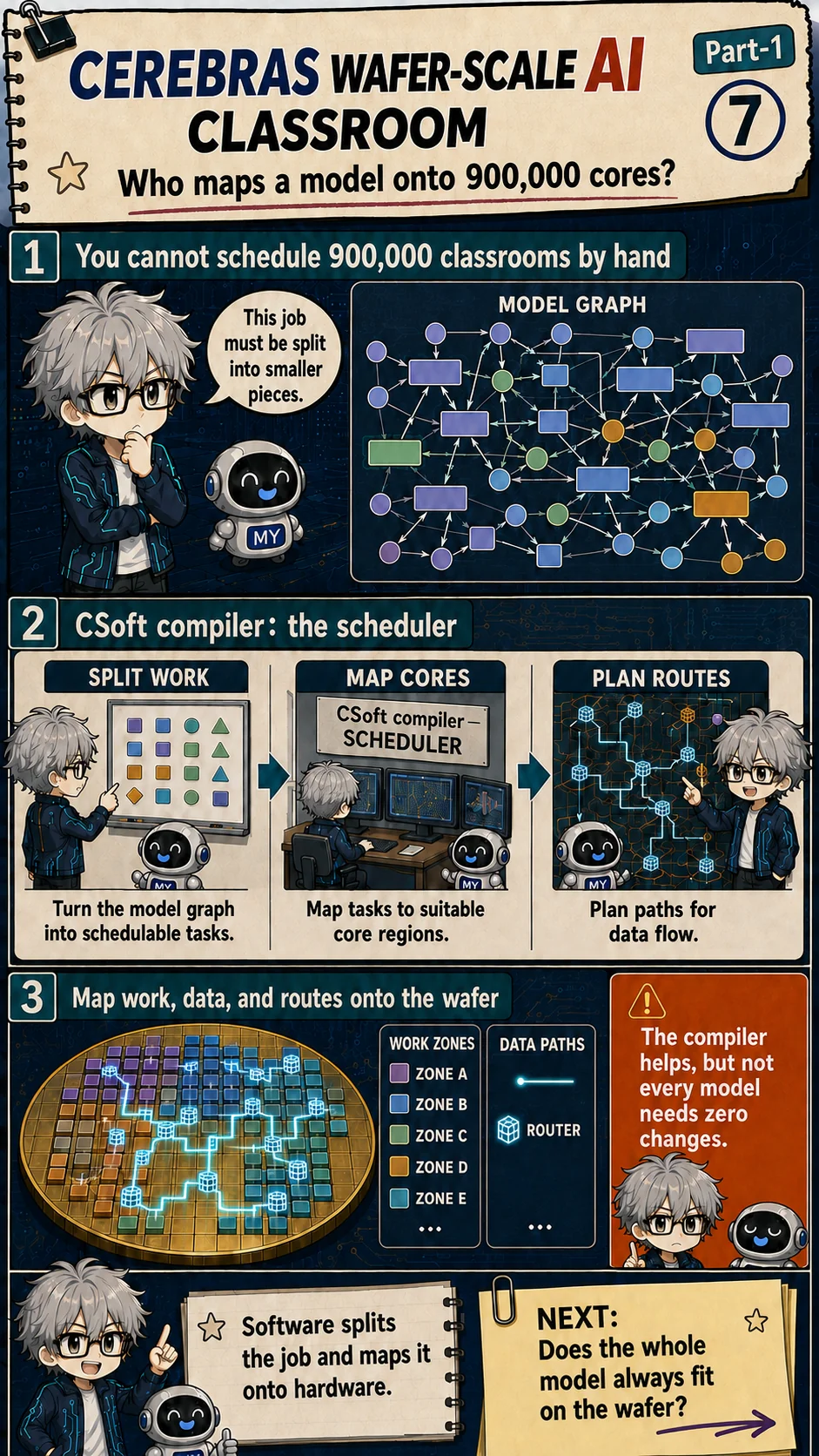
Who maps a model onto 900,000 cores?
Engineers cannot hand out jobs to 900,000 cores one by one. CSoft acts like a school scheduler: it reads the lesson plan, assigns work to classrooms, chooses where notes are stored, and plans the routes between them.
Take a tiny three-step graph: multiply an input by weights, pass the result through an activation function, then send it to the next layer. The graph records not only the operations, but also that step two must wait for step one.
The compiler partitions the graph into workable pieces, places computation and data on real PEs, routes messages between them, and schedules tasks when their dependencies are ready. Cerebras training documentation describes extracting an operation graph, matching kernels, and mapping work to the WSE. [4]
A good mapping keeps frequent partners close, balances local memory and network traffic, and avoids regions disabled after manufacturing test. A poor mapping can leave some PEs crowded and others idle, wasting impressive peak hardware.
This is hardware-software co-design. Hardware supplies cores, memory, and roads; software decides how to use them. A compiler still cannot guarantee that every framework, operator, tensor shape, and release will run unchanged or optimally.
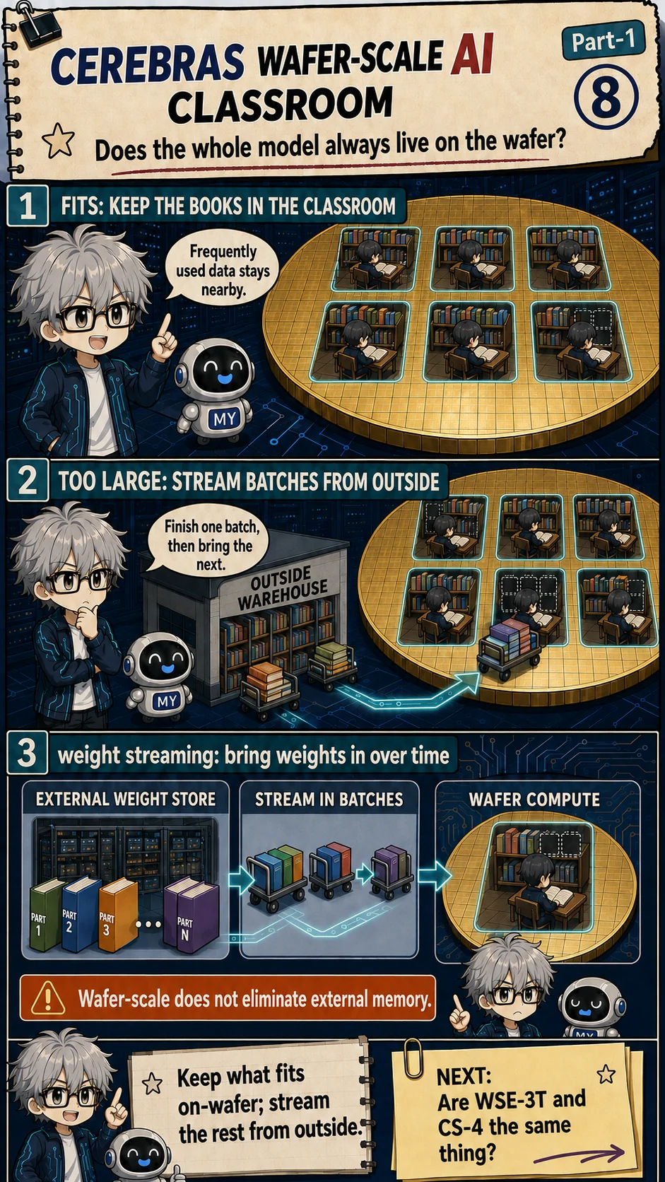
Does the whole model always live on the wafer?
'Does the model fit?' is not answered by counting weights alone. Inference also needs intermediate activations and a KV cache that grows with context and batch. Training adds gradients and optimizer state, so its memory ledger is different again.
Weights are learned parameters. Activations are intermediate results. Gradients say how weights should change, optimizer state remembers update history, and KV cache stores attention information for earlier tokens. They are different kinds of data, not one blob called model size.
If the working set fits in on-chip SRAM, more of it can remain near compute. If it does not, the system must partition, stream, or load it in stages. That is not automatically a failure; the real question is whether movement overlaps computation efficiently.
In an earlier Cerebras scale-out training design, MemoryX served as an external weight store. Layers were loaded onto the WSE one at a time, activations remained on the WSE, and computed gradients were sent back. [4]
With multiple systems, SwarmX broadcast weights and combined gradients. This allowed model capacity and compute capacity to scale somewhat independently rather than forcing both to grow in lockstep. [6]
Generations still matter. MemoryX and SwarmX belong to the established CS-2 scale-out story; CS-4 introduced Nexus, Direct Wafer Links, and disaggregated inference. They address related movement problems but are not the same component or an automatic one-for-one replacement. [5]
Engineer extension: residency is phase-specific
Model weights are only one part of the footprint. Training also needs optimizer state, gradients, and activations; inference adds KV cache whose size grows with batch and context. A claim that a model 'fits' must define the phase, precision, parallelism, and remaining runtime state.
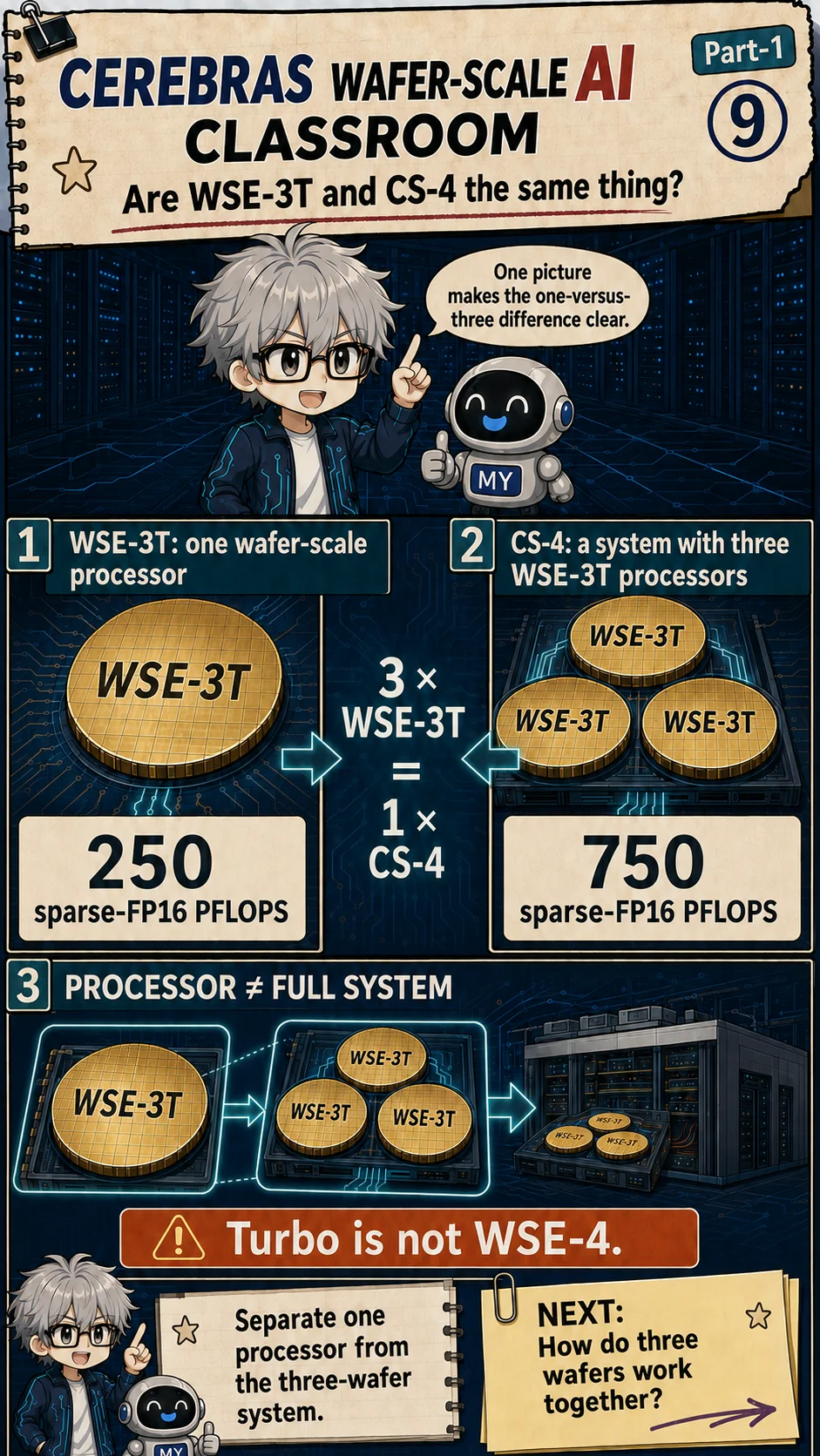
Are WSE-3T and CS-4 the same thing?
Keep the levels straight: WSE-3T is one wafer-scale processor, while CS-4 is a system containing three of them. It is the difference between one engine and a complete machine with three engines.
A FLOP is one floating-point operation. PFLOPS means 10 to the 15th floating-point operations per second. It resembles an engine's theoretical horsepower: useful for describing a ceiling, but not the elapsed time of a real trip.
FP16 means a 16-bit floating-point format. Sparse means the calculation takes advantage of zeros or other sparse structure. Precision, the sparse pattern, and which operations can be skipped are part of the claim.
Cerebras specifies 250 sparse-FP16 PFLOPS and 43.2 PB/s of memory bandwidth for one WSE-3T. Three wafers give CS-4 a listed total of 750 sparse-FP16 PFLOPS. The first distinction between 250 and 750 is one wafer versus three. [2]
Real model speed also depends on utilization, communication, shapes, software, and output conditions. Turbo names an accelerated WSE-3 variant in CS-4, not WSE-4. Undisclosed clock, process, TDP, or microarchitecture details should not be inferred from the label. [2]
Engineer extension: PFLOPS is not an application benchmark
Sparse-FP16 peak compute assumes a numeric format and sparsity condition. End-to-end throughput also depends on utilization, communication, memory behavior, sequence shapes, compilation, host overhead, and quality constraints. Compare matched workloads, not isolated headline numbers.
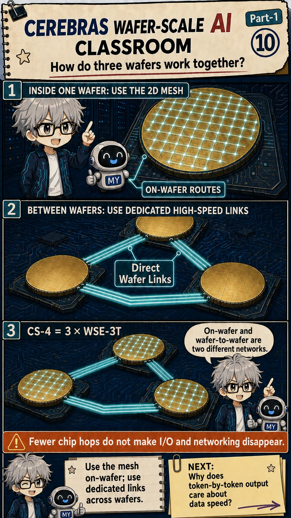
How do three wafers work together?
Inside one WSE, the 2D mesh acts like roads within a campus. To reach another WSE-3T, traffic uses a campus-to-campus highway: CS-4's wafer I/O subsystem and Direct Wafer Links.
Multi-wafer work begins with partitioning. Data parallelism can give different samples to different wafers. Model parallelism divides one model. A pipeline passes a stage's output to the next stage, like work moving down an assembly line.
Every boundary creates a handoff. Some steps must synchronize, and if one wafer takes 12 seconds while another takes 8, the faster one may still wait. Load imbalance can consume part of the expected speedup.
Cerebras reports wafer-to-wafer latency as low as two microseconds under its system conditions. That is a bounded vendor result, not a promise for every distance, configuration, and workload. [5]
Nexus separates Compute, Power, and I/O into modules for deployment and service. Modular hardware still has physical distance, synchronization, traffic, failure isolation, and retry work. [2]
Multi-wafer performance is therefore not just single-wafer performance multiplied by three. Links, partition choices, the slowest stage, and the effect of failures all shape the useful work delivered by the system.
Engineer extension: two network levels, two traffic models
The PE mesh handles fine-grained on-wafer traffic, while Direct Wafer Links carry partitioned work between WSE-3T processors. Partition boundaries, collectives, synchronization, and failure handling must be designed at the system level even when the link latency is low.

Why does token-by-token AI care about memory speed?
Suppose you ask, 'Why is the sky blue?' The model first reads the entire question and builds context for every token. That stage is prefill.
It may then produce 'Because,' add that token to the known context, and use everything so far to choose the next token. Repeating that step is decode.
Prefill has the whole prompt available and often exposes more parallel matrix work. It strongly affects time to first token: how long you wait before the answer begins.
Decode adds one token at a time but repeatedly uses model weights and the growing KV cache. Longer conversations and more simultaneous sequences generally require more cache, so data arrival can limit otherwise fast arithmetic.
Speed therefore has at least three meanings: time to first token, tokens per second after generation starts, and total requests served by the system. Low batch favors responsiveness; larger batches often favor aggregate throughput.
Model, precision, batch, prompt and output length, sparsity, software, and the comparison system all change results. Cerebras also states that its GPU comparisons vary with workload, configuration, date, and model. A fair number needs its test conditions beside it. [1]
Engineer extension: prefill and decode stress different resources
Prefill often exposes more parallel matrix work, while low-batch decode may be limited by repeated weight and KV traffic. Disaggregating the phases can specialize capacity and scheduling, but it adds handoff, queueing, and load-balancing questions. Any latency claim needs prompt length, output length, batch, model, precision, and percentile.
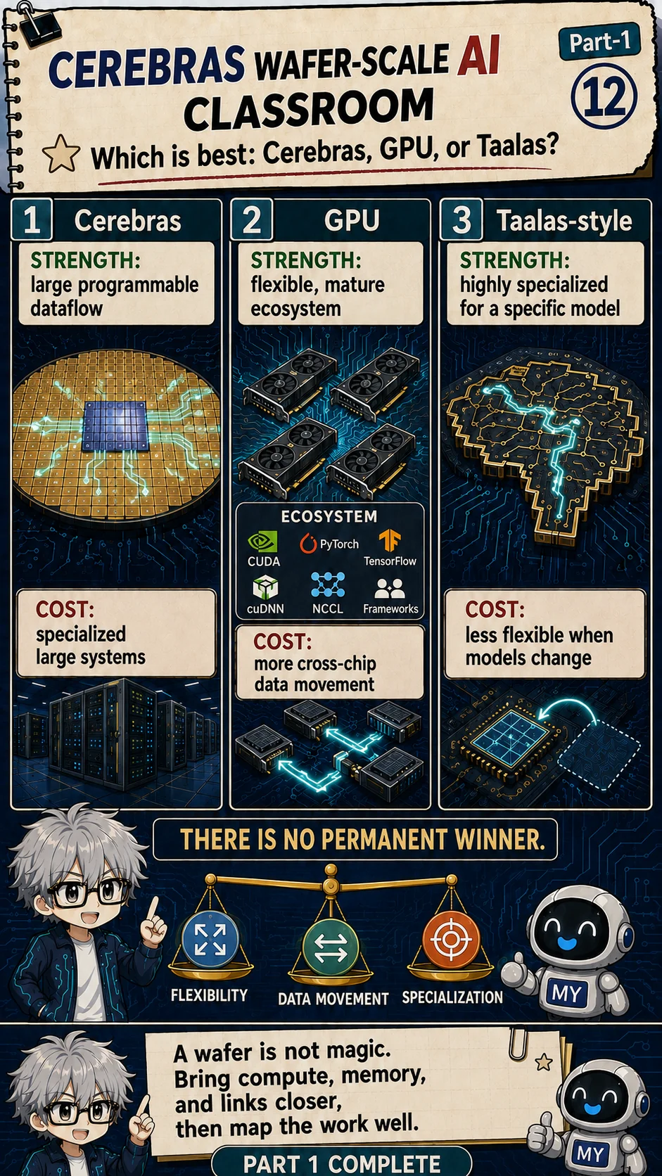
Which is best: Cerebras, GPU, or Taalas?
Imagine three campuses. Cerebras is a large integrated campus: compute, local memory, and on-wafer roads are close, while costs fall on a specialized system, cooling, power, and toolchain. A GPU cluster is a university town of standard buildings: flexible and broadly supported, but data travels through HBM, packages, and accelerator networks.
A Taalas-style design is a school built for one fixed curriculum. Putting model weights and data paths into silicon may reduce weight movement further, but changing the curriculum can become a new hardware project. It is a different direction from a programmable wafer-scale fabric.
Scenario one: a research group changes models, operators, and numerical formats every week. Software coverage, debugging, and reprogrammability may matter more than extreme specialization. GPU ecosystems often help here; Cerebras still has to support the target path.
Scenario two: a team is training an enormous model. The hard questions may be where model state lives, how systems synchronize, and whether utilization stays high. Cerebras weight streaming or multi-wafer designs are worth testing, but only with the real model and software release.
Scenario three: one stable model will serve huge inference volume for years. A hardwired design may trade flexibility for less weight movement and higher specialized efficiency, provided production volume can justify non-recurring engineering and model-change risk.
Use the same checklist every time: how often does the model change, what must remain resident, which batch, first-token latency, and throughput targets matter, what software is supported, and who pays for power, cooling, networking, service, and NRE? There is no permanent winner outside a workload.
Engineer extension: evaluate the whole product boundary
A fair architecture comparison includes compiler coverage, model-update cadence, power delivery, cooling, networking, availability, fault containment, observability, procurement, and NRE. A narrower silicon metric can be useful, but it cannot decide the system winner by itself.
References
- Cerebras, WSE-3T product page: Current WSE-3T scale, on-chip SRAM, and defect-tolerance description; performance comparisons remain vendor claims.
- Cerebras, CS-4 product page: Three-WSE-3T system composition, Nexus architecture, and single-wafer and system specifications.
- Cerebras SDK, Wafer-Scale Engine Architecture: Processing elements, local memory, 2D mesh, wavelets, task activation, and the programming model.
- Cerebras Training Docs, Weight Streaming Execution: MemoryX and weight-streaming background for the earlier scale-out training architecture.
- Cerebras, Introducing CS-4: Nexus, Direct Wafer Links, wafer I/O, and disaggregated inference positioning.
- Cerebras, Extreme-Scale AI Architecture: Original official description of the CS-2, MemoryX, SwarmX, and weight-streaming architecture.
- Gary Lauterbach, The Path to Successful Wafer-Scale Integration: The Cerebras Story, IEEE Micro (2021): The 525 mm² step-and-repeat field, offset wiring reticle, upper-metal-only field stitching, and wafer-scale yield strategy.
- Cerebras, Architecture Deep Dive: The sub-millimeter scribe crossing, high-level metal, parallel interface, million-plus cross-boundary wires, and auto-correction.
- Cerebras, Wafer-Scale AI, Hot Chips 2024: WSE-3's 84 die regions, cross-reticle fabric, extension to TSMC 5 nm through collaboration, and built-in redundancy.
Exercise: the fault remains; where does data go?
Choose source, destination and a disabled tile, then let BFS find an available shortest route. Step through each packet hop and try cutting an entire column. Redundant paths allow detours, not passage through every fault.
A custom 4×4 PE grid and store-and-forward packet model, not WSE routing, a reticle map, CSL simulation or clock performance. Each edge moves one wavelet per synthetic tick; the full packet arrives before the next hop. Concurrent traffic, buffers, virtual channels and backpressure are omitted. These counts cannot predict Cerebras latency.
Learning guide
AI Technology Classroom
Prerequisites
- Basic ideas of chips, memory, and AI inference; no semiconductor background is required
What I learned
- Explain why data movement can limit AI compute
- Trace how reticle stitching and redundancy make wafer-scale processing practical
- Separate WSE-3T processor specifications from the three-wafer CS-4 system
- Compare Cerebras, GPU clusters, and hardwired inference without a universal winner